
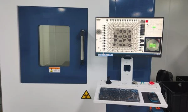
Board-level BGA underfill is material applied between a mounted package and its circuit board to support the solder-joint region. Consider it when a specific mechanical or thermal loading problem justifies the added material and process, and when the package manufacturer, assembly process and product qualification plan support its use. It is not a substitute for finding the cause of a defective joint.
Underfill can change how an assembly responds to load, but it also changes access for inspection and repair. The right decision depends on the package, board, material, process and service environment together. A successful trial on one combination does not automatically qualify another.
What is board-level BGA underfill?
A ball grid array connects to the board through solder joints under the package. Board-level underfill occupies some or all of the space between that mounted package and the PCB, depending on the material and process chosen. Capillary underfill, for example, is dispensed alongside a package and flows into the gap before cure. The actual coverage and cure requirements depend on the selected material and assembly.
Do not confuse this material with underfill already inside a flip-chip package, between its die and package substrate. Internal package construction does not establish what material, if any, should be added between that package and the board.
Underfill also has a different purpose and location from board-wide conformal coating or potting. Coating and potting decisions have their own environmental, access and qualification requirements; neither term establishes that solder joints beneath a BGA are reinforced.
Does every BGA need underfill?
No. Start with the exact component manufacturer's assembly and reliability instructions and the product's own loads. Texas Instruments' DSBGA Wafer Level Chip Scale Package application report, SNVA009AI, describes its DSBGA products as designed and tested for board-level thermal cycling without underfill in their intended applications. This is a wafer-level chip-scale package example; its statement applies to the identified product family and intended conditions, not to every BGA or every shock, bending or thermal exposure.
Underfill may be worth evaluating when a documented load threatens a joint region and the proposed material and process are compatible with the package. It is one candidate alongside changes to board support, enclosure constraints, component placement, handling or the joint design. The better option is the one demonstrated against the actual failure mechanism and product requirements.
How do you decide whether underfill addresses the problem?
Consider a hypothetical assembly with an intermittent BGA connection after enclosure installation. The symptom identifies an investigation area; it does not by itself establish a cracked solder joint, the cause of the damage or the need for underfill.
| Finding or question | Decision to make next |
|---|---|
| The net is intermittent, but the fracture location is unknown | Preserve the assembly and history. Localize the fault and select an examination that can distinguish solder, pad, trace and board-material damage. |
| The fracture is at a joint and installation loads the board | Compare enclosure support, fastener sequence and handling changes with a compatible reinforcement candidate. Define representative loading and acceptance criteria before building samples. |
| The damage is in the board material below a pad, or elsewhere in the circuit | Investigate that fracture path and its loading history. Do not assume filling the package gap will correct it. |
| A reinforced sample shows the same failure | Revisit the failure mechanism, process and test conditions. The result does not prove all materials or designs will behave alike. |
| A reinforced sample fails somewhere else, or the examination is inconclusive | Record the new failure location or uncertainty. The original symptom disappearing is not sufficient evidence that the whole product meets its requirements. |
Compare representative builds without and with the proposed underfill using the agreed process, sample plan, loading, inspection and acceptance criteria. Include the actual board support and other conditions that matter to the product. Keep the observation, interpretation and disposition separate.
For the assembly's handling history and possible support changes, see PCB handling and breakage prevention. A visible joint defect and an intermittent net can have different causes; solder joint defects and PCB pad cratering explain different fracture locations and investigation questions.
What must be checked before selecting a material?
Package instructions and geometry. Identify the exact component and revision, body size, ball pattern, standoff and any supplier restrictions. Check whether there is room to dispense and for the intended material flow, and whether nearby components, connectors or board features obstruct access. Edge reinforcement and material filling beneath a package do not necessarily produce the same coverage or performance; specify the intended placement and validate it.
Material properties and compatibility. Review the proposed product's data sheet for its intended use, flow behavior, cure conditions and relevant mechanical and thermal properties. Coefficient of thermal expansion and glass transition temperature are comparison inputs, not a universal pass/fail rule. Verify compatibility with the package, solder mask, surface finish, residues and other materials in the actual assembly. Ask the material and component suppliers about unresolved interactions.
Thermal and manufacturing history. Confirm that the package, board and adjacent parts can tolerate the complete planned process, including any preconditioning and cure, in addition to the preceding reflow cycles. Specify when cleaning, inspection, dispensing and cure occur. Follow the selected product's instructions; a temperature or time used for one material is not a general recipe for another.
Service and repair. Define the expected mechanical, temperature and environmental exposures and whether component replacement is required during manufacture or service. A material described as repairable is not proof that a particular device can be removed without board damage or that the rebuilt assembly meets the product requirements. Establish a validated repair and disposition route before production, or explicitly accept that affected assemblies may be non-repairable. The BGA board rework guide covers the removal and site decisions that may be affected by underfill.
What should the assembly process and inspection plan show?
Agree the sequence with the assembler and material supplier. Before dispensing, establish how the joint region and the assembly condition will be assessed, including any cleaning and residue requirements. Once cured material restricts access, some examinations or repair operations can become more difficult. Inspecting beforehand is useful, but it does not replace verification of the completed process.
The process plan should identify the material and revision, storage and usable-life controls, dispensing location, planned coverage, cure profile, and controls for the actual package and board geometry. Record the relevant lot and processing history so a change in material, package, board construction or process can be assessed against the original qualification.
Define what each inspection can and cannot detect. A visible fillet at the package edge does not by itself prove complete internal coverage. Imaging or other inspection may help assess features depending on the assembly, equipment and method, but a normal image does not establish every joint or interface is sound. Agree the locations, resolution, interpretation, acceptance criteria and any destructive confirmation needed for the project.
Qualification should address the finished assembly under representative conditions, not just whether the adhesive cured or the board passed an initial electrical test. An electrical pass establishes that the tested electrical criteria were met under the applied test conditions; it does not prove future reliability under every load.
What should you send with an underfill request?
Provide the assembly partner with:
- The exact component part number and revision, package instructions, land pattern, board stackup and relevant drawings.
- Package-to-board gap information, available dispense access, nearby parts and keep-outs, solder mask and surface finish.
- The known failure evidence or design load, product environment, intended service life and applicable qualification requirements.
- Existing soldering, cleaning and rework history, process constraints and any restrictions on heat or materials.
- The candidate material, if already selected, and the required coverage, cure, inspection, traceability, repair and reporting expectations.
- The proposed comparison builds, test conditions and acceptance criteria, including who will approve changes and final disposition.
Ask which processes and evidence the supplier can provide for this particular assembly. The material supplier's data describe its product; the assembler must establish the process for the build, and the product owner remains responsible for system qualification and release. APTPCB offers PCB fabrication and turnkey PCB assembly. Share the design and requirements with a PCB assembly quote request and confirm whether the proposed underfill, inspection and verification work is available for the project.
Frequently asked questions
Can underfill repair a cracked BGA solder joint?
No. Underfill is not a repair for an already cracked joint or an unidentified board defect. Investigate the failure and follow the applicable repair and acceptance requirements before considering any additional reinforcement.
Can an underfilled BGA be reworked?
Sometimes, but the answer depends on the material, package, board construction and qualified repair process. Confirm removal, site preparation, replacement, inspection and final acceptance for the particular assembly. A claim that a material is reworkable does not guarantee an undamaged repair or a qualified product.
Technical references
- Texas Instruments, DSBGA Wafer Level Chip Scale Package, AN-1112, SNVA009AI. Its underfill guidance concerns TI DSBGA products; check the instructions for the actual device and application.
- Texas Instruments, Flip Chip Ball Grid Array Package Reference Guide, SPRU811A. Figure 1 illustrates underfill inside a flip-chip package, distinct from material added between the package and board.