
PCB pad cratering is separation at a copper pad and the adjacent resin-weave composite, or cracking within the composite immediately next to the pad. A crack can exist while the solder joint still looks intact and the circuit still passes an electrical test. To investigate it, locate the fracture relative to the solder, pad and laminate, then compare that physical evidence with the assembly's loading and process history.
A lifted pad, an open net or a cracked solder joint is a reason to investigate, not a diagnosis by itself. The same assembly can have more than one kind of damage. For a broader view of defects and inspection choices, see common PCB defects; for fractures within the joint itself, see solder joint defects.
Where does pad cratering occur?
The layers of interest run from the component and solder joint to the copper land, then into the resin and glass-reinforced material below it. In pad cratering, the fracture can run at the pad-composite interface or within the adjacent composite. A pad may come away carrying some of that material; an early crack may remain hidden under a still-attached pad.
This is different from a crack through solder, separation at a solder or finish interface, a copper trace fracture, or separation elsewhere between board layers. The damage can occur together. Identifying the fracture path narrows the investigation, but it does not establish which event initiated it or whether the assembly is acceptable for service.
What should you do before removing the component?
Preserve the failed assembly and record its condition before rework, scraping, prying or repeated flexing. Those actions can create or extend damage and make the original fracture harder to interpret.
Record the board and assembly revisions, lot and serial numbers, component location, affected net, symptom and test conditions. Photograph both sides and mark the suspect area. Collect the known sequence of reflow, rework, depaneling, fixture contact, connector insertion, fastening, transport and service events. Note where the history is unknown rather than filling the gap with an assumed cause.
Retain representative unaffected assemblies or pads with known histories for comparison. Agree which specimens can be consumed by sectioning or mechanical testing and keep others unaltered where possible. A controlled electrical check may help localize an intermittent connection, but deliberately flexing a failed board can change the evidence; agree the purpose and limits with the investigation team first.
Which observation should guide the next step?
| Observation | What it can suggest | Next question for the investigation |
|---|---|---|
| An intermittent BGA net changes with handling | A connection may be opening under load, but the fracture could be in the solder, copper or board material. | Can the net and package location be localized without additional damage? What history and comparison samples are available? |
| A copper land separates with resin or glass-like material attached | The fracture may have traveled into the board material. | Examine both mating surfaces and the adjacent pad and trace. Did removal or testing alter the fracture? |
| A pad appears lifted or the exposed surface looks relatively clean | Separation may be close to an interface, but appearance alone does not identify the entire fracture path. | Inspect the separated surfaces and a suitable section; look for mixed paths and preparation artifacts. |
| A crack is seen within solder or through a trace | The observed path is in that conductor or joint. A second, hidden fracture is still possible. | Examine the board-side land and adjacent material where the history and risk justify it. |
| A selected cross-section shows no crack | That section did not reveal one at the examined plane and resolution. | Did the plane pass through the suspect location? Would another plane or specimen answer the question? |
Keep the report's observation separate from its interpretation. For example, “material is present on the underside of the separated land” is an observation; “depaneling caused the crack” needs supporting process and fracture evidence.
What can each inspection or test establish?
Visual examination and microscopy document exposed surfaces, cracks and fracture morphology. They cannot directly show every interface under an intact component. Keep detached material and document its orientation and location.
Electrical and functional tests can locate an open or intermittent circuit under the applied conditions. A passing result does not rule out a crack that has not interrupted the conductive path or that closes when unloaded.
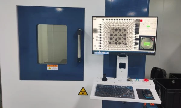
X-ray can help investigate hidden solder joints and other features, depending on equipment, views and interpretation. A normal image does not establish that the thin material beneath every land is sound. An image finding still needs to be related to the suspected failure location.
Cross-section and microscopy expose a selected plane through the joint, pad and board. This can show where an observed crack runs, but sectioning is destructive and may consume the selected specimen or part of the assembly; a plane can miss a localized crack. Agree the target net, section direction, preparation and reporting with the laboratory; note any artifacts or uncertainty. See PCB microsection analysis for sample selection and interpretation.
Dye-and-pry can help map separated locations across a package, but it changes the assembly. Prying can initiate or extend cracks. Dye penetration and the subsequent separation require careful interpretation: a separated surface alone does not prove when every crack began. Preserve comparison samples and agree how the lab will distinguish observations from conclusions.
Pad pull or shear tests apply a specified load to a prepared land or joint. Report the failure mode as well as the force: a result governed by solder or attachment failure answers a different question from a fracture in the laminate. Geometry, preparation, loading and conditioning matter. A coupon result supports a comparison under its stated conditions; it does not automatically predict the life of the finished product.
Board or assembly bending and shock tests can investigate response to chosen loading conditions. They may produce several failure modes, so pair electrical results with physical examination. The fixture, direction, rate, support and prior processing history must be relevant to the question being asked. A strain measurement records exposure at its measurement location; it is not by itself a universal pass/fail limit for every assembly.
How do you move from fracture location to cause?
In a hypothetical return, an assembly has an intermittent connection at a BGA after enclosure installation. A section through the affected location shows a crack at the pad-composite interface or within the adjacent composite. That supports a pad-cratering classification at the examined location; it does not prove installation was the first damaging event.
Compare the return with other assemblies and the recorded history. Check whether the same location is associated with rework, depaneling, fixture loading or connector and enclosure forces. Review board construction and package geometry alongside those events. If the team proposes a fixture or support change, evaluate it under representative conditions and check the resulting fracture modes, not just whether one board passes a bench test.
The PCB handling and breakage prevention article addresses support, separation and other controls before damage occurs. Material data and pad-strength comparisons can contribute to an investigation, but a higher glass transition temperature alone does not establish resistance to cratering in a particular design.
What should a failure-analysis request include?
Provide the laboratory or supplier with:
- The board and assembly revision, stackup and material information available, package and land pattern, lot, affected net and failure map.
- Photographs, electrical symptoms and test conditions, plus assembly, rework, handling and service history, including unknowns.
- Failed and suitable comparison samples, their traceability, and any restrictions on destructive examination.
- The question to answer, proposed section location or other examination, reporting format, specimen disposition and expected turnaround.
- The applicable drawing, contractual requirements and agreed acceptance or qualification criteria. Confirm which organization will perform each examination and supply each report.
IPC-9708's public introductory material describes test methods for assessing susceptibility to pad cratering. The public excerpt does not supply a project-specific acceptance decision. Agree the applicable revision, test conditions and project criteria with the relevant parties. The product owner remains responsible for disposition and product qualification.
APTPCB offers PCB fabrication and turnkey PCB assembly. When requesting a PCB or assembly quote, share the design, expected mechanical and thermal history, and required evidence. Confirm the investigation scope and deliverables for the project before relying on any particular test or report.
Pad cratering FAQ
Can a passing electrical test rule out pad cratering?
No. A crack can be present without interrupting the circuit under the test conditions. Physical examination and an investigation suited to the failure location may still be needed.
Is replacing the component enough to repair a cratered pad?
Not necessarily. Replacing the component does not by itself establish the condition of the underlying board material or adjacent conductor. Assess the damage and follow the applicable repair and acceptance requirements before returning the assembly to service.
Technical references
- Xie, Shangguan and Kroener, Pad Cratering Evaluation of PCB. The paper discusses fracture location and material, pad and assembly-level tests; its examples do not define acceptance criteria for a particular product.
- IPC, IPC-9708 public table of contents and introduction. Confirm the document and revision required for the project.