
Use HDI when a conventional PCB construction cannot meet the BGA escape, layer, electrical and assembly requirements within a supplier-approved process. Do not decide from ball pitch alone: compare practical routing candidates against the same pin map, stackup constraints and verification needs.
The choice affects both manufacturing cost and the connections available between layers. For those details, see HDI PCB cost and blind and buried via planning.
Why pitch alone does not answer the HDI question
A BGA’s ball pitch sets part of the available routing space, but it does not describe the complete escape problem. Two packages with the same pitch can have different pin assignments, usable routing paths, power and ground needs, and electrical constraints.
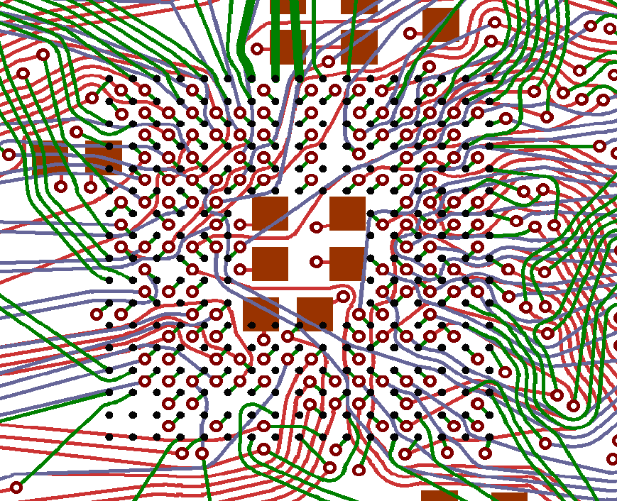
Example BGA routing layout. The image alone does not establish its via construction or stackup.
Before selecting a via structure, consider:
- Ball map and pin functions. Signal, power, ground, no-connect and reserved balls affect which routes must leave the package area and where they can go.
- Routing geometry. Pads, clearances, trace widths and any permitted neck-downs must work together under the intended fabrication process.
- Layer functions. A route is not useful if it requires sacrificing the reference plane or power distribution needed by the design.
- Electrical behavior. Impedance, return paths, crosstalk and via transitions may constrain an otherwise geometrically possible escape.
- Manufacturing and assembly. Via placement, land construction, solderability and thermal exposure must fit the proposed processes.
Texas Instruments’ AM62Lx Escape Routing Guidelines, SPRADI2, shows that plated through-holes can be used for a particular device and pin pattern without microvias. That is useful evidence that a conventional escape deserves consideration; it is not evidence that a different BGA will work the same way.
AMD’s UG1099 layer-count guidance likewise identifies package, pitch, pinout, routing width and fabrication technology as inputs. Where a design needs trace neck-down, review it with both the fabricator and the signal-integrity team rather than treating it as a free space-saving option.
Compare escapes using one set of requirements
Keep the component, pin map, electrical requirements and assembly assumptions fixed while comparing PCB constructions.
Hypothetical comparison
Suppose a design team is evaluating a BGA with a constrained board outline and several signals that need defined reference paths. The team has not yet established whether the breakout requires HDI. It prepares three candidates:
- Conventional candidate: plated through-holes and routing on the available signal layers.
- Limited HDI candidate: shorter blind via spans where needed for the escape, while retaining a conventional approach elsewhere.
- More complex HDI candidate: additional layer-to-layer transitions, potentially including stacked or staggered microvias, if the first two candidates cannot satisfy the requirements.
These are candidates, not predicted results. For each one, record the following:
| Review item | What to establish |
|---|---|
| Routing completion | Can every required connection leave the BGA and reach its destination without violating agreed geometry or electrical rules? |
| Layer use | How many signal layers are needed, and are the intended power and reference layers still usable? |
| Plane disruption | Do via clearances, antipads and transitions interrupt return paths or create unwanted congestion? |
| Via spans | Which layer pairs require connections, and are those spans compatible with the proposed stackup and build sequence? |
| Land construction | Are any vias in solderable pads? If so, what fill, cap, finish and inspection requirements apply? |
| Electrical review | Do impedance, return-current paths, transitions and any neck-downs satisfy the design requirements? |
| Feasibility and evidence | Will the supplier accept the construction, and what inspection or representative reliability evidence is needed? |
After the supplier reviews feasibility, choose a candidate that meets the requirements with the least necessary complexity. The fewest layers are not always the best choice: a construction can save layers but leave unacceptable reference-plane breaks or unresolved assembly risks.
Work from the ball map to the layer architecture
A good first pass separates the connections by function. Identify which balls need routing, which connect to power or ground, and which are reserved or otherwise constrained by the device documentation. Check whether the package has recommended breakout or placement guidance before assigning a stackup.
Then establish a provisional layer plan:
- Assign likely signal, reference and power functions to layers.
- Identify where important signals need continuous reference paths.
- Map the required transitions between layers.
- Examine whether the BGA escape consumes space needed by other components, planes or routes.
- Review the resulting architecture with the fabrication supplier.
A stackup is more than a layer count. Copper and dielectric arrangement, materials, thicknesses, impedance targets and via spans interact. A change made to create another escape route can also change the electrical environment or the feasible manufacturing sequence. The PCB stackup design guide provides a starting point for documenting those layer decisions.
Do not wait until routing is complete to ask whether the stackup can be built. A supplier may propose a different construction or identify a detail that requires a layout change. Bring those questions forward while alternative escapes are still practical.
Select via spans for the connection, not the label
A via span states which layers a connection reaches. That information is more useful in an RFQ than simply asking for an “HDI board.”
Plated through-holes
A plated through-hole connects through the board thickness. It can be a practical BGA escape option when the pad arrangement, routing channels, layer plan and electrical requirements allow it.
Its full-depth presence also has consequences. Through-hole clearances occupy space on layers the signal may not use, and the transition may leave an unused via portion relevant to the electrical design. Evaluate those effects in the context of the actual signal and stackup; do not assume that every through-hole is either harmless or unsuitable.
Blind and buried vias
A blind via connects an outer layer to an internal layer. A buried via connects internal layers without reaching an outer surface. Used appropriately, they can make space available on layers that a full-depth hole would otherwise occupy.
That benefit comes with construction decisions. The requested spans must fit the layer sequence, and different span combinations can affect how the board is built. Show each required layer pair explicitly. If a candidate relies on multiple transitions to complete one connection, include the complete path rather than listing the holes independently.
Stacked and staggered microvias
Some escapes may require transitions across more than one layer interval. Depending on the construction, microvias can be arranged in a stack or offset from one another.
Neither arrangement is a universal reliability answer. Geometry, materials, build process and thermal exposure matter. Ask the supplier to review the actual configuration and provide the agreed evidence appropriate to the application. If the layout can use more than one arrangement, compare their routing, plane and construction effects before deciding.
The IPC-hosted paper Microvia Reliability Failure Modes discusses construction-dependent failure mechanisms and representative coupons. It is useful background for asking better questions, but the 2009 paper is not itself a current mandatory IPC standard.
Treat via-in-pad as a fabrication and assembly decision
Placing a via in a BGA land can create routing options where space is limited. It also changes the requirements for the solderable land. The designer, fabricator and assembler need a shared understanding of the intended surface and the processes that will follow.
For each via-in-pad location, document:
- The land and via geometry, including the layer span.
- The required via fill and cap construction, as agreed with the supplier.
- The surface finish and solderable-land requirements.
- The inspection and acceptance criteria for the finished feature.
- The assembly thermal exposure the PCB is expected to see.
Do not assume that a note saying “via-in-pad” fully defines the construction. Likewise, do not specify a fill or cap by habit without confirming that it suits the land, stackup and assembly process. The via planning guide can help turn those choices into explicit fabrication information.
Protect signal paths while creating routing space
An escape can look complete on a routing layer while introducing an electrical problem elsewhere. Review the trace, its reference, each transition and the destination together.
Pay particular attention to:
- Reference continuity. Check what happens to the return path as the signal leaves the package and changes layers.
- Plane interruptions. Review via clearances and dense breakout areas for cuts or narrow paths in reference and power planes.
- Impedance. State the required targets and tolerances for relevant structures, and check whether the proposed stackup supports them.
- Neck-downs. Identify their locations and geometry, then obtain supplier and signal-integrity review where needed.
- Transitions. Consider the electrical effect of the actual via path and any unused portion of a through-hole.
- Coupled routes. Verify that differential or other coupled signals can maintain their required geometry through the escape and transitions.
An impedance coupon or TDR report, if part of the agreed verification plan, should be interpreted against the defined stackup and test conditions. It does not automatically establish that every route or the finished product meets its requirements. See how to read an impedance coupon TDR report.
Build verification around the actual construction
A technically plausible drawing is not the same as evidence that a particular construction is suitable for its use. Agree on what will be checked and what evidence is needed before releasing the design.
For the PCB fabrication scope, ask the supplier to confirm feasibility of the proposed stackup, spans, land construction and relevant geometries. Agree on inspection and acceptance requirements for the features that matter to the design. Where reliability evidence is required, ask how representative it is of the actual stack, via construction, materials and expected thermal history.
Assembly adds another set of conditions. Communicate the expected thermal exposure and solderable-land requirements, and coordinate the fabrication details with the assembly process. A fabrication inspection result alone does not establish that assembly will be successful.
Finished-system qualification is a separate activity. PCB or assembly acceptance does not by itself establish performance over the product’s intended use and environment. The project team should define any system-level qualification needed for that use case.
Where standards or device documents are part of acceptance, identify the applicable document and revision in the project requirements. Do not substitute an assumed universal microvia limit, stack count or cycle count for supplier-approved construction and project-specific validation.
Prepare an RFQ that lets the supplier evaluate the design
An actionable HDI RFQ describes both the board and the decisions that remain open. Include the following where applicable:
- Package information: device identification, package drawing, ball map and relevant device recommendations.
- Design data: current layout and fabrication files, with critical areas and any unresolved breakout options identified.
- Layer architecture: proposed stackup, layer functions, board thickness requirements and material requirements.
- Via information: required layer spans, via-in-pad locations, proposed stacked or staggered arrangements, and fill and cap requirements.
- Electrical requirements: impedance targets and tolerances, relevant structures, and any areas requiring special transition or neck-down review.
- Surface and quantity: finish, quantity and other order requirements needed to assess the build.
- Assembly exposure: expected assembly thermal history and solderable-land needs.
- Acceptance: applicable documents and revisions, inspection requirements, and any reliability evidence required for the use case.
Ask the supplier to respond with feasibility feedback, its proposed construction, any required design changes, and the inspection and representative evidence that can be agreed for the project. If a requirement is still undecided, mark it as an open question rather than leaving the supplier to infer it.
When the breakout comparison and RFQ package are ready, you can request a quote from APTPCB or contact APTPCB with the proposed construction and open questions. For an overview of the board category, see HDI PCB.