
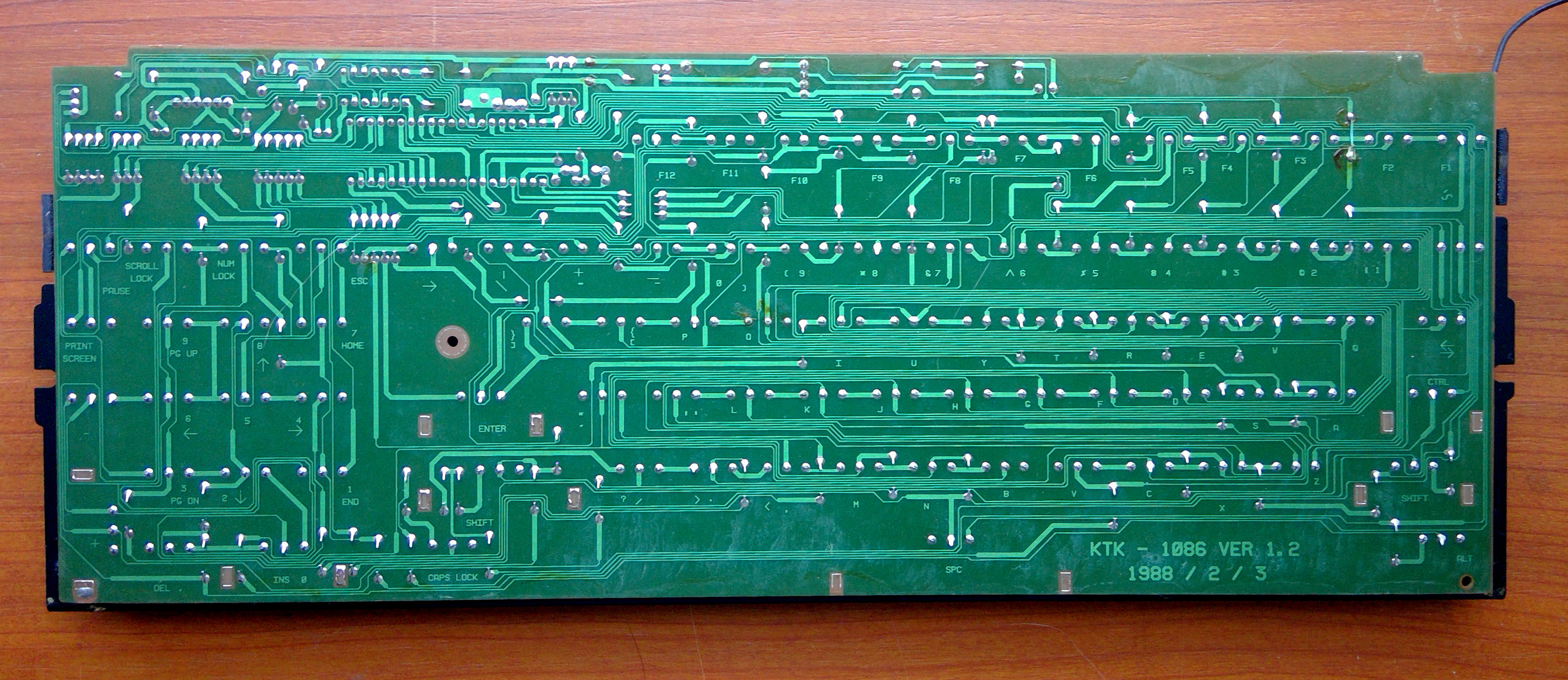
The physical layout of a keyboard PCB determines where keys fit. Its matrix connects the switches to the controller, and the firmware turns those readings into key events. Before ordering, make sure all three describe the same keyboard.
An example keyboard PCB. Component choices and board layouts differ by design.
For a custom mechanical keyboard, the most useful design sequence is:
- Fix the key positions and mechanical constraints.
- Choose switches, mounting method and stabilizers.
- Map each switch to a matrix and controller pin.
- Configure the firmware to match the circuit.
- Separate the files and work needed for board fabrication, PCB assembly and final keyboard assembly.
Start with the mechanical layout
Place the switches using the drawings for the exact parts you intend to use. Check their orientation and footprint against the key layout, especially around larger keys that need stabilizers.
The PCB also has to fit a larger mechanical stack. Before release, check the following together rather than as independent parts:
- Switch and, if used, hot-swap socket footprints and orientation
- Stabilizer locations and clearances
- Plate openings and support
- Board thickness and its interaction with the chosen parts
- Case mounting points and internal clearances
- Connector position and access through the case
For example, Kailh’s CPG151101S11-16 socket drawing and CPG1511F01S06 switch drawing are references for those exact parts, not for every socket or switch. Use the relevant manufacturer drawings for your own selection, then verify the stack with a prototype.
Soldered or hot-swap?
A soldered design connects the switches to the PCB as part of assembly. A hot-swap design uses compatible sockets installed on the board, allowing switches to be inserted separately. The choice changes both the footprint and the assembly plan.
For hot-swap, check socket placement and orientation against the switch drawing, and decide who supplies and installs the sockets. In either design, assess how the plate, case and PCB support the switches. Don’t assume that changing the footprint alone establishes a workable mechanical assembly.
Design the matrix and choose the controller together
A key matrix connects switches between row and column nets. Firmware scans those nets to identify which positions are active. This can reduce the number of controller I/O lines needed compared with assigning a separate input to every switch, but it also means the schematic and firmware must agree on the mapping.
Choose a controller after counting the I/O needed for the matrix and any other planned functions. Also review the actual interface, firmware support, power and protection requirements for the design. A controller’s presence in another keyboard project does not establish that it supports your pin assignment or firmware configuration.
Ghosting and diode direction
Without isolation, a combination of pressed switches can create an unintended path through a matrix. The scanner may then register a key that was not pressed; this is ghosting. For example, three pressed switches at three corners of a two-row, two-column rectangle can create a path that appears to activate the fourth corner.
A diode in series with each switch can prevent those matrix ghost paths when its polarity and the scan circuit are designed consistently. Diode direction is not universal: it must match the schematic’s current path and the selected firmware scan convention.
Preventing matrix ghost paths is also not the whole definition of N-key rollover (NKRO). What the keyboard can report depends on the hardware, firmware and host. Treat rollover as a behavior to verify for the finished design, not as a consequence guaranteed by adding diodes.
Worked example: a four-key matrix
The following is a hypothetical mapping, not a measured result. Imagine four keys arranged in two physical rows and two columns. The controller scans active-low rows one at a time; columns have pull-ups, and unselected rows are high-impedance.
In this chosen circuit, each path runs from the column through the switch and diode to the row. The diode anode faces the switch/column side, and its cathode faces the row side. The firmware must be configured for that circuit and scan convention.
C0 o---[SW1]---|>|---o R0
C1 o---[SW2]---|>|---o R0
C0 o---[SW3]---|>|---o R1
C1 o---[SW4]---|>|---o R1
Each repeated label represents the same net: both C0 ends connect to column C0, for example. In this sketch, |>| shows each diode with its cathode bar toward the row. The controller scans the rows and reads the pulled-up columns; the exact controller pins are a separate choice.
| Physical location | Switch | Matrix position | Diode orientation | Firmware coordinate | Expected key event |
|---|---|---|---|---|---|
| Upper left | SW1 | R0, C0 | Anode toward C0; cathode toward R0 | (0, 0) | Q |
| Upper right | SW2 | R0, C1 | Anode toward C1; cathode toward R0 | (0, 1) | W |
| Lower left | SW3 | R1, C0 | Anode toward C0; cathode toward R1 | (1, 0) | A |
| Lower right | SW4 | R1, C1 | Anode toward C1; cathode toward R1 | (1, 1) | S |
Here, firmware coordinate (0, 1) is intended to read SW2 and emit W. That expectation still needs verification on the assembled prototype: a footprint rotation, swapped net, incorrect diode placement or firmware mapping error could produce a different result.
QMK’s How a Keyboard Matrix Works and configuration reference are useful primary sources for understanding matrix scanning and matching configuration to a chosen circuit. Consult the documentation for the firmware and version you actually select.
Check the schematic against the firmware
Before ordering, trace one switch through all three descriptions of the design:
- Schematic: SW2 connects column C1 to row R0 through its diode; check the diode symbol and footprint polarity together.
- Pin assignment: Record which actual controller pins connect to R0 and C1. The names
R0andC1in this example are net names, not MCU pin numbers. - Firmware: Assign the same pins and matrix scan direction in the chosen firmware. Confirm that matrix coordinate
(0, 1)maps to the intended key event. - Prototype: Press SW2 and verify that it produces W. Then test a relevant three-key combination, such as SW1, SW2 and SW3, and check that SW4 does not register by itself.
Repeat the single-key check for the other switches and record the actual results. The expected events in the table are a test plan, not evidence that a particular PCB or firmware has passed.
Route and review the PCB
Once the mechanical positions and matrix are stable, route the row and column nets and connect them to the intended controller pins. Keep the schematic, PCB designators and firmware mapping traceable to one another. Review connector routing, power connections and protection needs for the selected interface rather than copying them without checking the controller and system requirements.
The PCB design guide covers the broader layout process. For a keyboard, add checks that are specific to the product:
- Compare every switch footprint with its selected part drawing and physical orientation.
- Check diode polarity in the schematic, PCB footprint and assembly documentation.
- Confirm that switch, stabilizer, socket and connector clearances fit the plate and case.
- Check that controller pin assignments match the firmware matrix.
- Plan access for programming and the functional checks you want to perform.
A prototype is the practical point at which to check both fit and behavior. Proposed checks include inspecting diode orientation, confirming each key event, trying relevant multi-key combinations and checking connector and case fit. Record actual results separately from the expected mapping.
Define what you are ordering
A keyboard project can involve three distinct scopes:
- Bare-board fabrication: manufacture the PCB from the released board files and fabrication requirements.
- PCB assembly (PCBA): install the agreed electronic components on the board.
- Final keyboard assembly: bring together the PCB, switches or sockets, plate, stabilizers, case and other selected parts as agreed.
Do not assume that a request for one scope includes the others. Agree separately on component supply, installation and testing, including whether switches, sockets or connectors are part of the requested work.
For the board, prepare fabrication outputs and review them against the design. The guide to what a Gerber file is explains one part of that handoff. For PCBA, provide a clear BOM, component placement information and assembly drawings; see how to prepare a BOM for turnkey PCB assembly and assembly drawing essentials. Identify polarity-sensitive parts and any parts to leave uninstalled.
Before release, use the design for assembly checklist to review the package as a whole. If you need help defining the work, describe the desired fabrication, assembly and test scope when you request a quote, or contact APTPCB with the design questions you need resolved.