
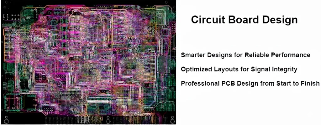
PCB design turns a schematic into a physical board that a factory can build and an assembler can populate. The work runs in a fixed order: capture the circuit, choose the board outline and stackup, place components, route connections, check the layout against manufacturing rules, and release a controlled set of files. Most respins come from decisions made out of that order, such as routing before the stackup is fixed or placing parts before the enclosure is known.
This guide walks through the PCB design process step by step and shows, at each stage, which manufacturing constraint you should check before moving on. It is an overview of the whole flow. For a line-by-line layout checklist, use the PCB layout DFM guidelines.
Key takeaways
- Circuit board design is a sequence of commitments. Fix the outline, stackup, and placement before detailed routing, because each later step depends on them.
- Pick your manufacturer's capability early and load it as your design rules. A clean DRC only proves the layout matches the rules you entered.
- Choose layer count from routing density, reference planes, and package escape, not from habit.
- Place for assembly as well as for signals: orientation, clearances, fiducials, test access, and thermal mass all affect yield.
- Run DFM checks on the generated outputs, not only on the CAD database.
- Release one controlled package: fabrication data, drill, stackup, drawing, netlist, and assembly data at matching revisions.
What is PCB design?
PCB design is the engineering work that defines a printed circuit board's copper pattern, layer structure, holes, outline, and assembly data. It starts after the schematic exists and ends when the manufacturing files are released. A good PCB layout meets electrical requirements (signal integrity, power delivery, EMC), mechanical requirements (outline, connectors, mounting holes, height limits), thermal requirements, and the process limits of the factory that will build it.
Schematic design and PCB layout are often done by different people. The schematic says what connects to what. The layout decides where every part sits and how each connection is made in copper. Both feed the same release package.
PCB design process step by step
The table below is the core of this guide. Each row is a stage of the PCB design workflow, the decision you make there, the manufacturing constraint to check before you commit, and the deliverable that should exist when the stage is done.
| Stage | Decision you make | Manufacturing constraint to check first | Deliverable at the end |
|---|---|---|---|
| 1. Requirements | Interfaces, power budget, operating environment, enclosure, quantity | Board class (for example IPC Class 2 or 3), target volume, assembly route | Written requirement list and mechanical envelope |
| 2. Schematic capture | Circuit, part choice, net names, reference designators | Part availability and package types the assembler can place | Reviewed schematic and a first BOM |
| 3. Footprints and libraries | Land patterns and 3D models for every part | Pad geometry suited to reflow or wave soldering; paste and mask openings | Verified footprint library |
| 4. Outline and mechanical | Board shape, mounting holes, connector positions, keep-outs | Edge clearance, panel method (V-score or tab routing), tooling holes | Board outline and mechanical DXF/STEP agreed with the enclosure |
| 5. Stackup and layer count | Copper layers, dielectric thickness, copper weights, impedance targets | Materials in stock, buildable dielectric pairs, finished thickness tolerance | Stackup proposal confirmed by the fabricator |
| 6. Placement | Component positions and orientation | Assembly clearances, fiducials, test access, heavy or tall parts, thermal balance | Placement frozen and reviewed |
| 7. Routing | Traces, vias, planes, length and impedance constraints | Minimum trace/space and drill for the chosen factory and copper weight | Fully routed layout with clean DRC |
| 8. Verification | DRC, ERC, SI/PI checks, design review | Manufacturer DFM review of generated outputs | Closed review list and approved exceptions |
| 9. Release | File set, drawings, revision control | Complete fabrication and assembly package with a manifest | Released package ready to quote |
You can loop back, and most designs do. The rule is that each loop should go back to the stage that owns the problem. A trace that cannot fit between two pins is usually a placement or stackup problem, not a routing problem.
How to choose layer count and stackup
Layer count is one of the largest cost and lead-time drivers in PCB design, so decide it with evidence:
- Package escape. Count the rows of BGA balls you must route out. Each inner signal layer escapes a limited number of rows at a given via size and pitch.
- Reference planes. Fast edges and controlled-impedance lines need a continuous reference plane next to them. A four-layer board with signal, ground, power, signal is a common starting point.
- Power distribution. Multiple supply rails may justify extra plane layers, or split planes on one layer if the currents and noise allow it.
- Isolation. Analog, RF, and high-current sections may need dedicated layers or extra spacing.
Once the count is chosen, the stackup defines dielectric thicknesses, copper weights, and which layers act as references. Agree it with the fabricator before routing impedance-controlled nets, because the trace widths depend on it. The PCB stackup design guide explains reference planning, and the impedance calculator gives first-pass trace geometry.
Some quick reference points for common choices:
| Layer count | Typical use | Stackup note |
|---|---|---|
| 2 | Simple controls, power, low-speed I/O | Hard to keep a solid reference plane under every signal |
| 4 | Microcontroller boards, mixed-signal, moderate speed | Signal / ground / power / signal is a common arrangement |
| 6 | Fast interfaces, more power rails, denser BGA escape | Allows two inner signal layers between planes |
| 8 and above | Large BGAs, many high-speed links, backplanes | Plan reference layers for every signal layer |
Placement rules for assembly
Placement decides most of what routing can achieve and almost everything about assembly yield. Keep these rules in view:
- Mechanical first. Lock connectors, switches, mounting holes, and anything that must align with the enclosure.
- Group by function. Keep each power stage, clock, RF section, and sensitive analog block compact, with its decoupling and support parts close to the IC pins.
- Keep orientation consistent. Aligned polarized parts reduce placement and inspection errors. Mark polarity clearly on silkscreen.
- Respect clearances. Leave space for nozzle access, rework, inspection, and solder fillets. Keep tall parts away from fine-pitch parts that need visual or AOI inspection.
- Plan fiducials and tooling. Global fiducials on the board or panel help machine alignment. Local fiducials help fine-pitch packages.
- Think about the second side. If parts go on both sides, keep heavy parts on the top side and confirm which bottom-side parts can survive a second reflow.
- Provide test access. Decide early whether the board will see flying probe, ICT, or functional test, and place test points accordingly.
The design for assembly checklist goes deeper into each of these.
Routing a PCB layout
Route in priority order: critical nets first (clocks, high-speed pairs, sensitive analog, high-current paths), then the remaining signals, then pours and stitching.
- Set width, spacing, and via rules per net class. High-current nets need width from a current and temperature-rise calculation. Impedance-controlled nets need geometry from the confirmed stackup.
- Keep return paths continuous. Avoid routing fast signals across plane splits or gaps.
- Use the smallest number of via types that solves the problem. Each added type (blind, buried, microvia, filled via-in-pad) adds process steps and cost.
- Balance copper across layers where you can; heavy imbalance can increase warpage.
- Leave the routing in a state the fabricator can verify: no unconnected copper islands unless intended, no acid traps, no slivers in pours.
For fast interfaces, the high-speed PCB design guide covers impedance, length matching, and crosstalk in more depth.
DFM checks before release
Design rule checks prove that the layout follows the rules you configured. They do not prove those rules match the factory, so run a design-for-manufacturing review as well. Check at least:
- Minimum trace, space, and annular ring against the factory's normal capability, not its absolute limit
- Drill sizes, aspect ratio, and hole-to-copper clearance
- Solder mask openings, mask webs between fine-pitch pads, and via tenting or plugging
- Copper to board edge clearance, especially near V-score lines
- Silkscreen clear of pads and readable after assembly
- Panelization, breakaway tabs, and fiducials if you deliver panels
- Footprints matched to the actual parts in the BOM
The PCB design review checklist is a usable template, and the design for manufacturing guide explains how fabrication, assembly, and test reviews fit together.
Files for a PCB quote
The last step of the PCB design process is the release. A complete package lets the manufacturer quote without guessing and build without engineering holds.
Fabrication files
- Gerber RS-274X or Gerber X2 for every copper, mask, paste, silkscreen, and outline layer, or ODB++ / IPC-2581 as an alternative
- NC drill files (Excellon) with plated and non-plated holes separated, plus a drill map
- Stackup with layer order, materials, copper weights, dielectric thicknesses, and finished thickness
- Fabrication drawing: board dimensions, tolerances, material, finish, mask and silkscreen colors, impedance table, and acceptance class
- IPC-D-356 netlist for electrical test comparison
Assembly files
- BOM with manufacturer part numbers, reference designators, and quantities
- Placement (centroid / pick-and-place) file with X, Y, rotation, and side
- Assembly drawing with polarity marks, special instructions, and do-not-place parts
- Test requirements if the supplier will run programming or functional test
Release checklist before you send it
- All files come from the same design revision and carry the same revision code
- Gerbers were checked in a viewer, not only exported
- Drill file units and format match the Gerbers
- Stackup and impedance table agree with the fabrication drawing
- BOM reference designators match the placement file
- Open DFM questions are closed or listed as approved exceptions
- A short readme lists every file and its purpose
You can preview your outputs with the online Gerber viewer before uploading them.
Why involve APTPCB before you release?
APTPCB's engineers can review a layout before or after routing, confirm whether the proposed stackup is buildable with stocked materials, and check the generated outputs against the fabrication and assembly route you plan to use. For prototypes on a tight schedule, quick turn PCB fabrication starts from that reviewed package. Incomplete data is the most common reason a quick-turn order loses days.
The review covers manufacturability. Electrical validation, EMC, thermal performance, firmware, and product certification remain with the design owner.
Relevant standards and references may include:
- IPC-2221 and IPC-2222: generic and rigid printed board design
- IPC-7351: land pattern design for surface mount components
- IPC-2581: data transfer format for board and assembly data
- IPC-6012: qualification and performance of rigid printed boards
- IPC-A-610: acceptability of electronic assemblies
Frequently asked questions
What are the steps of PCB design?
The usual steps are requirements, schematic capture, footprint creation, board outline and mechanical definition, stackup selection, component placement, routing, verification (DRC, DFM, design review), and release of fabrication and assembly files. Each step should be stable before the next one depends on it.
How long does it take to design a PCB?
It depends on complexity. A small two-layer board can be laid out in days, while a dense multilayer board with BGAs and high-speed interfaces can take weeks, plus review cycles. Freezing requirements and placement early shortens the schedule more than faster routing does.
What is the difference between PCB design and PCB layout?
PCB design often refers to the whole job, from schematic to released files. PCB layout is the physical part of that job: placement, routing, planes, and copper geometry. Many teams use the terms interchangeably.
Which software is used for PCB design?
Common tools include Altium Designer, Cadence Allegro and OrCAD, Siemens Xpedition and PADS, and KiCad. Any of them can produce a manufacturable board if the design rules match the fabricator and the outputs are checked before release.
What files does a manufacturer need from a PCB design?
A fabricator needs Gerber or ODB++/IPC-2581 data, NC drill files, a stackup, a fabrication drawing, and ideally an IPC-D-356 netlist. An assembler also needs a BOM, a placement file, and an assembly drawing. All files should share one revision.
When should I ask the manufacturer to review my PCB design?
Ask before routing if the board uses controlled impedance, HDI, rigid-flex, heavy copper, or unusual materials, so the stackup and rules are confirmed early. Ask again after outputs are generated to catch export and documentation errors.
Design in the order the factory builds
A PCB design succeeds when each decision is made at the right stage and checked against the process that will build it. Fix the outline, stackup, and placement before detailed routing, load real manufacturing rules, verify the generated outputs, and release a single consistent package. That is the shortest path from schematic to a board that works on the first build.