
Assess conductive anodic filament (CAF) risk when a PCB has closely spaced internal conductors that will experience both moisture and electrical bias. The assessment should represent the actual conductor geometry, material system and manufacturing history—not just cite a laminate’s CAF-resistant designation.
There is no universal clearance or test profile that establishes safety for every design. A useful program asks which biased paths are credible, how the construction could change in production and assembly, and what evidence would distinguish an internal failure from a surface problem.
What CAF is—and what it is not
CAF is an internal electrochemical failure mechanism. A common path develops along a glass/epoxy interface when absorbed moisture and electrical bias are present. The resulting conductive path can reduce insulation resistance between conductors and eventually create a short.
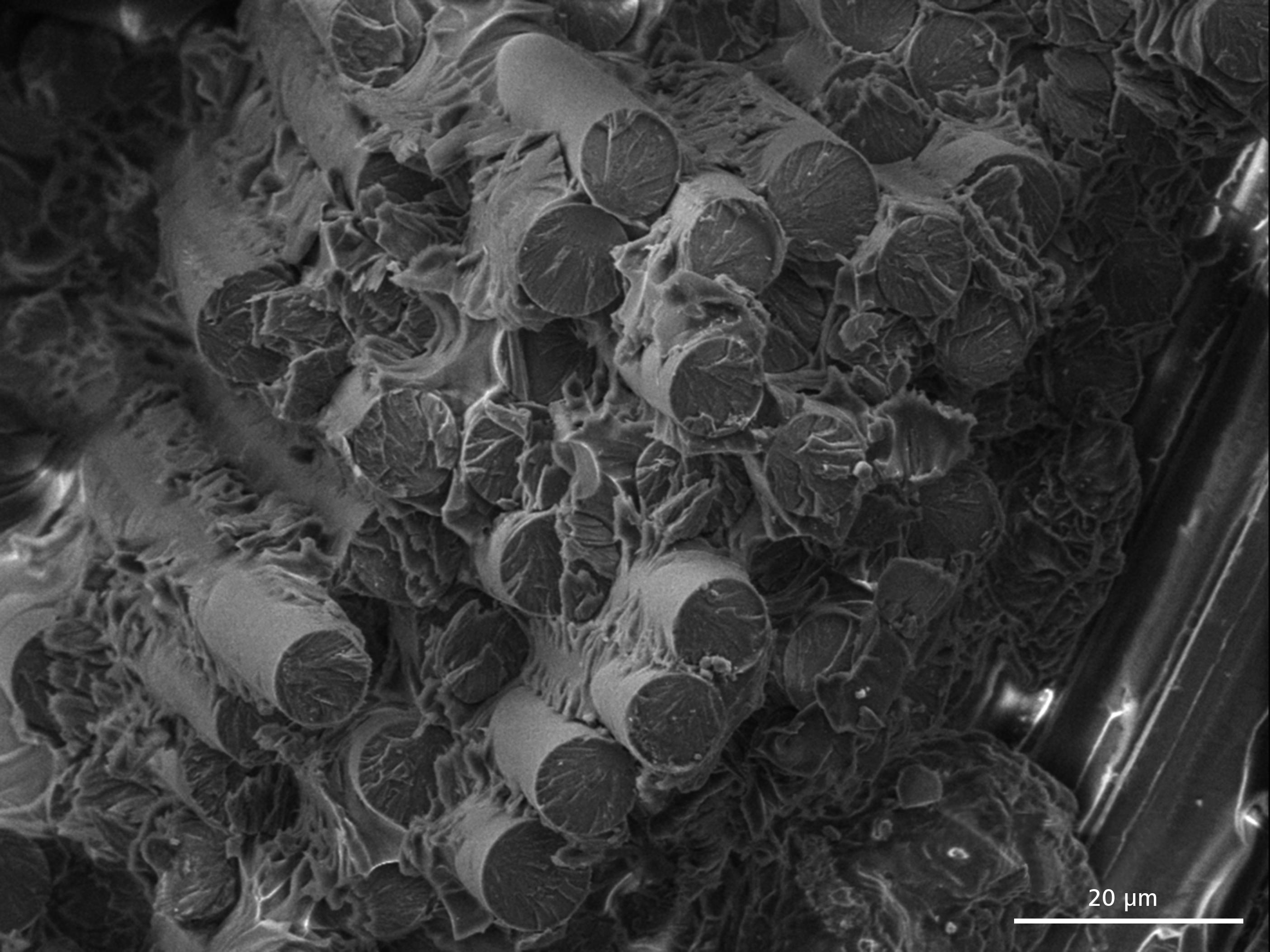
A low-resistance reading alone does not prove CAF. Other internal defects can cause a short, and surface electrochemical migration has a different surface or assembly mechanism. Diagnosis therefore needs electrical history, construction details and physical examination rather than a single resistance measurement.
Material selection matters, but it is only one part of the decision. For example, Isola’s 370HR datasheet describes that named material as CAF resistant. That statement does not establish the performance or service lifetime of a particular fabricated stackup.
For background on material selection and documentation, see FR-4 material properties, what copper-clad laminate is, and the stackup documentation guide.
Decide which conductor paths to assess
Start with conductors that can have a sustained potential difference in the intended environment. Then identify the smallest credible manufactured separation, including relevant tolerances, rather than relying only on the nominal design drawing.
| Biased geometry | Physical question | Evidence to request or review |
|---|---|---|
| Hole to hole | Could adjacent plated holes be closer in production than the nominal spacing suggests? | Hole locations and tolerances, stackup, relevant drill and fabrication history, and a representative test pattern |
| Hole to plane | How close can the plated hole come to an internal plane at the manufactured clearance? | Plane clearance and its tolerance, layer position, hole details, polarity and representative test geometry |
| Other internal conductor pairs | Is there a credible biased path through the dielectric between the conductors? | Layer construction, separation, material system, actual bias and the reason the selected pattern represents the product |
| Surface conductors | Could moisture or assembly conditions support a surface path rather than an internal one? | Surface condition, assembly history, electrical observations and a separate surface-migration assessment where appropriate |
The tightest nominal gap is not automatically the only important geometry. Consider the applicable voltage and polarity, exposure, the amount of product represented by the pattern, and what manufacturing variation could do to the separation.
Hypothetical example: hole to hole versus hole to plane
A design has adjacent plated holes on different nets, as well as a plated hole passing near an internal power plane. The hole-to-hole spacing appears tighter on the drawing, so the team initially plans to test only that pattern.
During review, the team finds that the hole-to-plane clearance has a different manufacturing tolerance and remains biased in the intended operating state. The responsible engineer and lab decide whether both patterns need representation, using the credible manufactured separations and actual polarity—not the nominal spacing alone.
This example establishes no ranking between the two geometries. The decision is to document why each path is included or excluded.
What can a team change before release?
Start with the biased paths that have the least credible manufacturing margin. A change is useful only when its effect on the complete design and build is understood.
| Decision | Action to consider | What to check before accepting it |
|---|---|---|
| Geometry | Move a biased hole or adjust a plane clearance to increase the relevant dielectric separation. | Recheck routing, current return paths, other clearances, tolerances and the actual hole-to-plane and hole-to-hole distances. |
| Material | Compare a specified laminate and prepreg construction with a candidate that has documented CAF test evidence. | Compare the test vehicle, geometry, fabrication history and conditions behind the evidence. Also check electrical, thermal and supply requirements; the material name alone is not board qualification. |
| Fabrication | Review drilling, hole-wall preparation and lamination controls with the board fabricator. Damage or separation at a glass/resin interface can create a potential migration path. | Ask which records or inspection results are available for the proposed build and how a process or material change is communicated. Do not assume a particular factory process or test is included. |
| Product environment | Review how enclosure conditions and operating modes affect moisture exposure and the duration and polarity of bias. | Consider both normal use and likely excursions. Surface protection may reduce some exposure but does not, by itself, establish resistance to an internal path. |
The chosen action may change a coupon or qualification plan. Agree with the product engineer and fabricator which construction will be tested and how later substitutions will be evaluated. Thermal exposure during assembly can also be relevant to interface condition; PCB thermal expansion provides context without turning a laminate CTE value into a CAF prediction.
Choose the method for the suspected mechanism
IPC-TM-650 2.6.25C, dated February 2021, covers internal migration. Its section 1 warns that the method was not designed for use above 100 V DC. Confirm the applicable current revision and discuss any intended use outside the method’s scope with the lab and responsible product engineer.
IPC-TM-650 2.6.14.1, dated September 2000, specifically concerns surface migration. It is not interchangeable with the internal-migration method. A surface issue on an assembled board may require a different investigation from an internal path through the laminate.
The method reference is a starting point, not a substitute for a project-specific agreement on exposure, bias, observation and acceptance. Fabrication or assembly evidence also does not by itself qualify the complete system for its service environment.
Build a practical test request
The product team should identify which items below are contractual requirements and which are questions for the lab to resolve. Do not leave an unspecified test profile or pass criterion to be inferred from a material datasheet.
State in the request or contract:
- Scope and purpose: the product or construction represented, the intended decision, and whether the work evaluates a coupon, a board or another agreed specimen.
- Construction and history: named laminate and prepreg materials, stackup and relevant manufacturing history, plus assembly or reflow history where applicable.
- Geometry: conductor pairs and layer positions, worst credible separations, manufacturing tolerances and the rationale for the selected patterns.
- Exposure and electrical conditions: the project-specific moisture exposure, applied bias and polarity, including how these represent actual use.
- Controls and observations: agreed control specimens, resistance observation intervals and how an interruption or failure will be recorded.
- Sample plan and acceptance: sample size, pass criterion and how the result will support the stated decision. Agree these before testing rather than adopting an assumed universal criterion.
- Report deliverables: specimen identification, conditions and history, raw resistance versus time, failures and their timing, and microsection or other examination outcomes.
- Change review: which changes to material, stackup, geometry, fabrication, assembly or exposure require the assessment to be reviewed.
Ask the lab and responsible product engineer:
- Does the proposed pattern represent the credible hole-to-hole and hole-to-plane paths, including tolerances?
- Are the controls sufficient to help interpret the effect of bias and exposure?
- Is the selected method applicable to the intended bias, and what limitations should be reported?
- What examination is practical after a resistance drop, and what can or cannot be concluded from it?
- Is the sample plan adequate for the decision, rather than merely convenient to run?
A dedicated pattern can make the assessment easier to interpret, but its relevance must be justified against the product construction. See PCB test coupons for context on representing a design in a test specimen.
Triage a low-resistance path
- Preserve the evidence. Record the affected nets, measured resistance, bias and polarity, exposure, observation time and specimen identity. Retain the resistance-versus-time record rather than reporting only the final reading.
- Check the measurement and history. Review connections, controls, test interruptions, manufacturing records and any assembly or reflow history before assigning a cause.
- Locate the likely path. Determine whether the evidence points toward an internal conductor pair, a surface path or another defect. Compare the location with the intended test geometry and credible manufacturing variation.
- Plan the physical examination. Coordinate sectioning and other examination with the lab so that the suspected path and relevant layers are represented. Record both positive observations and examination limits.
- Report the conclusion with its uncertainty. IPC-TM-650 2.6.25C notes that forensic microsection detection can be difficult. Failure to observe a filament is therefore not conclusive evidence that CAF did not occur; likewise, a resistance drop alone does not prove it did.
- Review the design and assessment. If the path or history differs from the assumed worst case, revisit the geometry, controls, material and process records, and the need for further project-specific testing.
The most useful outcome is a traceable decision: what construction was assessed, which failure mechanism the evidence supports, and what remains uncertain before the product team makes its next qualification decision.
For an APTPCB quotation or project discussion, provide the stackup, relevant layer and hole geometry, operating bias and environment, and any test or documentation requirements. Confirm the scope of any proposed material, fabrication or test support for the specific project.