
A four-layer PCB usually has four layers of copper, not four total layers of material. Insulating material separates the copper, and the finished board may also have solder mask, printed markings and surface finish. Those physical materials matter, but they are not counted as additional copper layers.
A PCB design file can contain even more “layers”: copper artwork, solder mask openings, paste apertures, board outlines and other instructions. Some describe materials that remain on the board; others tell a fabrication or assembly partner how to process it.
For a basic introduction to the board itself, see what is a PCB. When ordering a multilayer board, the distinction matters because a correct layer count alone does not tell a fabricator which file belongs at each position, what each copper layer does or how the layers connect.
Copper count versus physical construction
Copper layers carry the board’s electrical features: traces, component pads, planes and other copper areas. A layer can contain signal routing, a ground plane, power distribution, or a combination. The count refers to distinct copper levels in the board, not to the number of nets or individual copper shapes.
The insulation between copper layers is dielectric material. In a rigid PCB, construction may include:
- Core: cured insulating material, commonly supplied with copper foil bonded to one or both sides.
- Prepreg: partially cured resin-reinforced material that can bond layers together during multilayer lamination.
- Copper foil and plated copper: conductive material patterned to form the circuitry.
- Solder mask and legend: coatings applied to the board surface, where specified.
A normal two-copper-layer rigid board can begin with a copper-clad core: copper on each side of the insulating core. It does not inherently need a separate prepreg layer between each foil and the core. Multilayer constructions can use prepreg to bond cores and other layers together. The actual material arrangement depends on the agreed stackup and manufacturing process.
Likewise, a four-copper-layer board has more than four physical material regions. Calling it “four-layer” is useful shorthand for copper count, but it is not a complete construction specification.
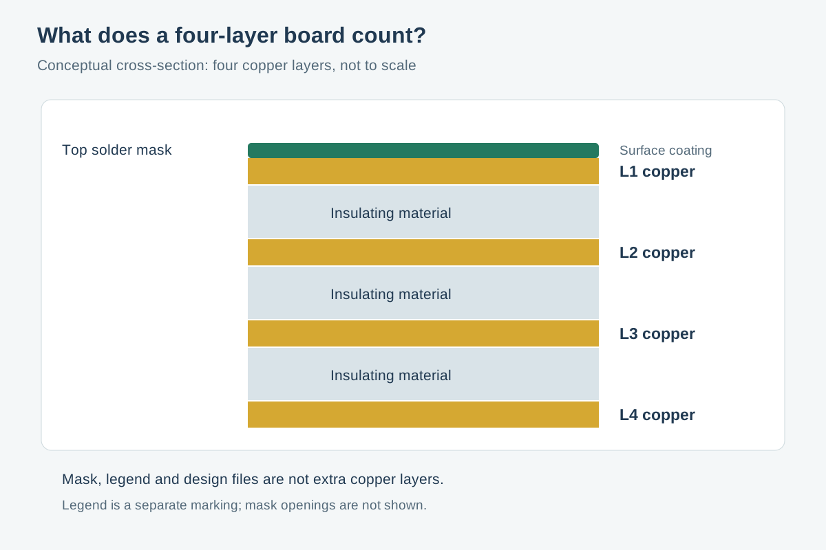
Conceptual illustration, not to scale or a specification for an actual board. Copper count, insulating material and design-output layers describe different things.
A hypothetical four-copper-layer example
Assume a rigid board has four copper layers, numbered from top to bottom:
| Copper ID | Hypothetical function | What still needs confirmation |
|---|---|---|
| L1 | Top-side signals and component pads | Connections, copper features and reference requirements for the actual design |
| L2 | Ground plane | Plane continuity, clearances and the nets that connect to it |
| L3 | Power distribution, signal routing, or both | Actual net assignments and whether the copper provides a suitable reference where needed |
| L4 | Bottom-side signals and component pads | Connections, routing and reference requirements for the actual design |
This is an invented reference example, not a universal stackup recipe. Another four-layer board may assign these functions differently. The names in the design, their physical order and the intended connections must be confirmed for the particular board.
A four-layer arrangement can offer more routing space and opportunities to place reference copper near signal layers than a two-layer arrangement. It does not, by itself, prove acceptable electromagnetic interference, signal integrity or impedance. Those outcomes depend on factors including geometry, dielectric properties, return paths, discontinuities and the finished construction. A nearby plane is useful only when it supports the intended return path.
For controlled-impedance work, provide the applicable traces, target values and tolerances along with an agreed stackup; do not infer a guarantee from “four-layer.” The PCB stackup design article addresses the construction choices in more detail.
How vias relate to the layers
A plated through-hole via can pass through the board, but passing through a copper layer is not the same as connecting electrically to it. At each layer, the design determines whether the via connects to a pad or copper area, or is isolated by clearance.
In the hypothetical example, a via might join a signal on L1 to a signal on L4 while remaining clear of L2 and L3. A different via might connect ground copper where the design calls for it. Review the actual net and layer geometry rather than assuming that every via joins all four layers.
Blind or buried vias have different start and end layers. If a design uses them, communicate those endpoints and requirements explicitly; four copper layers do not automatically imply that such vias are present or agreed.
Mask, legend and paste: different jobs
Solder mask is a real coating, usually applied to the outer board surfaces. Its openings expose selected copper features, such as pads, for subsequent processing and assembly. Exposed copper may receive a specified surface finish; an opening should not be interpreted as a requirement to leave bare copper.
Mask is not a substitute for a copper drawing. A mask opening identifies where coating should be absent; the copper artwork defines the conductive feature. An unintended opening can expose copper that was meant to remain covered, while a missing opening can cover a pad intended for soldering. See what is solder mask for more context.
Legend, often called silkscreen, is also a physical marking when applied. It may show reference designators, polarity indicators or other identification. It is not an electrical copper layer. If a marking conflicts with a pad or opening, resolve the intended treatment before release rather than relying on an assumption about what will be removed.
A paste layer generally describes aperture information for a solder-paste stencil. It is primarily an assembly output, not a permanent bare-board layer. During assembly, paste is deposited through stencil apertures and reflowed; the paste artwork itself is not a coating laminated into the PCB. A board or side with no applicable surface-mount paste requirements may not need a paste file, but that should be made clear to the assembly recipient.
The distinction is also reflected in KiCad’s Pcbnew Layers documentation, which separates copper, mask, paste, legend and other design-layer purposes.
Map each file to its recipient
The following is an illustrative transfer map for the hypothetical four-layer board above. File names are examples of descriptions, not required naming conventions. Confirm the actual names and formats with each recipient.
| Output or information | Purpose in this example | Recipient and review condition |
|---|---|---|
| L1 top copper | Top pads and signal copper | Board fabricator; confirm it is the first copper layer and matches the top-side view. |
| L2 copper | Ground copper | Board fabricator; confirm layer position, net assignment and via clearances. |
| L3 copper | Power and/or signal copper | Board fabricator; specify the actual function and confirm it is not confused with L2. |
| L4 bottom copper | Bottom pads and signal copper | Board fabricator; confirm layer position and orientation against the other files. |
| Top and bottom mask | Areas where solder mask is to be opened | Board fabricator; check that the files correspond to the correct sides and intended exposed features. |
| Top and bottom legend | Component and other printed identification | Board fabricator; identify any side with no legend and check for conflicts with openings. |
| Top and/or bottom paste | Proposed stencil aperture information | Assembly or stencil recipient; identify applicable sides and review aperture requirements. It is not an additional copper layer. |
| Board outline | Finished perimeter and relevant routed features | Board fabricator; make the intended contour unambiguous and distinguish it from other mechanical lines. |
| Drill and slot information | Hole locations and applicable hole types | Board fabricator; identify plated and non-plated requirements and any special via endpoints. |
| Stackup and fabrication drawing | Copper order, construction requirements and supporting notes | Board fabricator; reconcile these documents with the artwork and any controlled-impedance requirements. |
The table is not a substitute for a complete fabrication or assembly package. For example, the outline identifies the shape, but hole tolerances, finished thickness, surface finish and other requirements may need separate specification. The fabrication drawing essentials article provides a starting point for that handoff.
What a cross-section can—and cannot—show
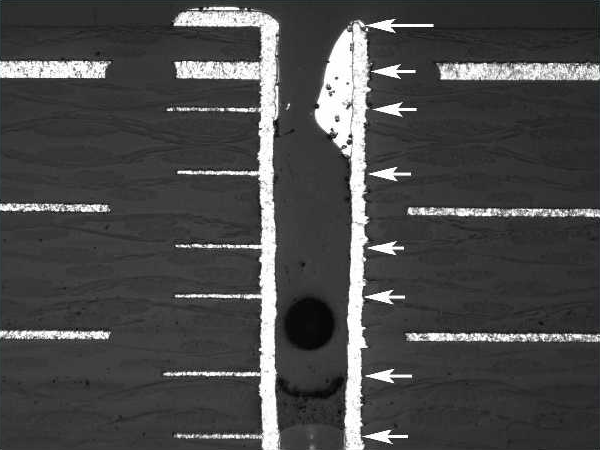
NASA/GSFC coupon through-hole microsection by Charles E. Powers, 2009. The original arrows indicate missing annular rings. No scale is provided; this image does not establish the board’s total layer count, acceptance status or any APTPCB work. Image credit and source record.
A microsection shows a cut through a particular region of a board or coupon. It can help an inspector examine features visible at that location, but this image is not a general layer-count diagram. In particular, the absence of a visible feature at one cut location should not be used to reconstruct the whole board or determine acceptance without the applicable design and inspection criteria.
Example: a reversed or misnamed layer package
Invented review scenario: A purchaser receives a four-layer package with files named L1-top, L2-ground, L3-power and L4-bottom. The drawing also says four copper layers, but a review suggests that the file named L1-top contains the pattern expected on the bottom.
Do not resolve that conflict by trusting the file name, the viewing color or a single screenshot. Colors and display conventions are not universal, and a bottom-side view can appear different depending on how it is presented.
A practical review is:
- Hold the release and identify the reference view. Ask the designer which side is considered the top and how the artwork is intended to be viewed. Do not assume a file needs mirroring merely because it looks reversed in a viewer.
- Compare distinctive features across outputs. Check an unambiguous connector, keyed feature or component pad pattern against the intended top and bottom copper, mask, legend and assembly information. Check alignment with the outline and drill locations.
- Verify the inner copper order separately. A correctly identified top file does not prove that L2 and L3 are in the right order. Compare the layer list and stackup with the actual copper content and intended nets.
- Resolve electrical consequences. If an inner layer appears mislabeled, check via connections and clearances against the design intent. Simply swapping two file names could create incorrect connections or invalidate the intended reference arrangement.
- Issue a corrected package. Have the design owner identify the authoritative files and layer order, revise the conflicting output or documentation, and communicate the new revision to every recipient. Remove or clearly supersede the earlier package.
If the designer cannot establish which output is authoritative, stop and request clarification before fabrication. A board can have the correct number of copper layers and still be wrong because the artwork, order or connectivity was miscommunicated.
Before requesting fabrication
For an efficient review with APTPCB, identify the copper count and provide the files together with a layer map, stackup requirements and fabrication notes. State any features that need special agreement, such as controlled impedance or non-through vias. For assembly, separately identify paste and other assembly outputs and their intended recipients.
If the package is ready, use the quote request. If the layer mapping or requirements are uncertain, contact APTPCB before treating the files as released.
Public source references
- KiCad, Pcbnew Layers.
- NASA, PCB fabrication presentation, NASA Technical Reports Server record 20190001381.
- NASA/GSFC, Charles E. Powers, 2009 coupon inspection image, NASA Technical Reports Server record 20090027819; see the linked image credit and source record above.