
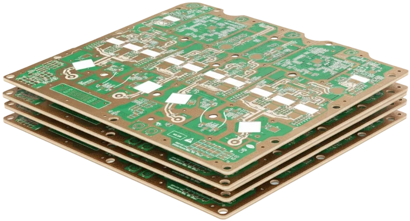
PCB stands for printed circuit board. A PCB is a flat, layered part that holds electronic components in place and connects them with copper paths instead of loose wires. The copper is bonded to an insulating base, usually glass-reinforced epoxy called FR-4, and patterned so that each trace runs only where the circuit needs a connection.
A bare PCB has no components on it. Once parts are soldered to it, the result is a printed circuit board assembly, or PCBA. That difference matters when you ask for a quote, because a board house, an assembler, and a box-build supplier deliver very different things.
This guide explains what a circuit board is made of, what each part of a PCB does, the main types of PCB, and how to decide which type your product needs before you send files to a manufacturer.
Key takeaways
- The PCB meaning in electronics is "printed circuit board". Older documents sometimes say PWB (printed wiring board) for the same bare board.
- A typical rigid PCB is a stack of copper foil and glass-epoxy dielectric, finished with solder mask, silkscreen, and a solderable surface finish on the exposed copper.
- The parts of a PCB you can see are traces, pads, vias, planes, solder mask, silkscreen, and the board outline. Components are not part of the bare board.
- Board type follows the product's constraints: layer count from routing density, flex or rigid-flex from motion and packaging, metal core or ceramic from heat, special laminates from frequency.
- A PCB becomes a PCBA only after components are placed, soldered, inspected, and tested. Decide early whether you are buying the bare board, the assembled board, or a finished unit.
What does PCB stand for?
PCB stands for printed circuit board. "Printed" refers to the way the copper pattern is created: an image of the circuit is transferred onto copper-clad material, and the unwanted copper is etched away. Modern factories use photoresist and laser direct imaging rather than ink printing, but the name stuck.
Two other terms describe the same object or a close relative:
| Term | What it means | When you will see it |
|---|---|---|
| PCB (printed circuit board) | The bare board with copper, dielectric, mask, and finish | Most datasheets, CAD tools, and quotes |
| PWB (printed wiring board) | Older term for the bare board | IPC documents, defense and legacy drawings |
| PCBA (printed circuit board assembly) | A PCB with components soldered on | Assembly quotes, EMS contracts |
| CCA (circuit card assembly) | Same as PCBA | Aerospace and defense programs |
If you searched "PCB meaning" from a chemistry or environmental context, note that PCB also stands for polychlorinated biphenyl, an industrial chemical. That is unrelated to circuit boards.
What is a circuit board made of?
A circuit board is made of alternating conductive and insulating layers bonded under heat and pressure. On a standard rigid board, the ingredients are:
- Copper foil. It forms traces, pads, and planes. Thickness is usually given in ounces per square foot. 1 oz copper is roughly 35 µm thick, and many boards use 0.5 oz to 2 oz. Power boards can go much heavier.
- Dielectric (substrate). FR-4 is the common choice: woven fiberglass impregnated with flame-retardant epoxy resin. A rigid "core" is fully cured laminate with copper on both sides. "Prepreg" is glass cloth with partially cured resin that bonds cores and foils together during lamination.
- Plating. Holes are drilled through the stack and plated with copper so that layers can connect to each other.
- Solder mask. A polymer coating, most often green, that covers copper you do not want solder on. It reduces solder bridges and protects traces from oxidation and handling damage.
- Silkscreen. White or black legend ink for reference designators, polarity marks, logos, and part outlines.
- Surface finish. A thin coating on exposed copper pads that keeps them solderable. Common options are lead-free HASL, ENIG, ENEPIG, OSP, immersion silver, and immersion tin. The PCB surface finishes guide compares them by assembly and storage needs.
Other substrates replace FR-4 when the design needs them: polyimide for flex circuits, aluminum or copper bases for heat spreading, ceramic for high power density, and PTFE or hydrocarbon laminates for RF and microwave signals.
How does a circuit board work?
Current flows through the copper paths that connect component pins. The dielectric keeps neighboring paths apart. On multilayer boards, whole copper layers act as power and ground planes. They distribute supply voltage, give fast signals a clean return path, and help spread heat. Vias carry signals and power between layers. The board itself does not compute anything; it is the wiring, the mechanical carrier, and often part of the thermal and electrical design.
Parts of a PCB
These are the main parts of a circuit board you will see in a layout file or on a finished board.
| Part of a PCB | What it does | What to define in your files |
|---|---|---|
| Traces | Carry signals and power between pads | Width, spacing, copper weight, impedance targets if any |
| Pads (lands) | Copper areas where component leads are soldered | Footprint geometry, finish, mask opening |
| Vias | Plated holes that connect layers | Drill size, type (through, blind, buried, microvia), fill or tenting |
| Planes | Large copper areas for power and ground | Layer assignment in the stackup |
| Plated through holes | Holes for through-hole leads and press-fit pins | Finished hole size and tolerance |
| Solder mask | Insulating coating over copper | Color, clearance, dam rules |
| Silkscreen | Printed legend | Reference designators, polarity, orientation marks |
| Board outline | Final shape, slots, cutouts | Profile layer, tolerances, panel method |
| Fiducials | Optical targets for assembly machines | Location and clearance |
The components themselves (resistors, capacitors, ICs, connectors) are mounted on the pads during assembly. If you need help naming and identifying them, see the guide to SMT component polarity marks.
PCB layers
A single-sided board has copper on one side. A double-sided board has copper on both sides, connected by plated holes. A multilayer board has three or more copper layers, typically an even number such as 4, 6, 8 or more, with inner layers buried inside the laminate. The arrangement of copper and dielectric is the stackup, and it controls impedance, crosstalk, and how the board behaves during reflow. The PCB stackup design guide covers how to plan it.
PCB types compared
There are several kinds of PCB, and most products use one of the types below. They differ in construction, cost, and the problem they solve.
| PCB type | Construction | Typical applications | Main trade-off |
|---|---|---|---|
| Single-sided | One copper layer on FR-4 or CEM | Power supplies, LED strips, simple controls | Routing space; jumpers may be needed |
| Double-sided | Two copper layers with plated holes | Consumer devices, instruments, industrial I/O | Limited room for planes and controlled impedance |
| Multilayer | 4 or more copper layers laminated together | Processors, networking, mixed-signal boards | More lamination steps, longer lead time |
| HDI | Microvias, fine lines, often sequential lamination | Phones, wearables, compact compute modules | Higher cost per layer and more process steps |
| Flex | Copper on polyimide film | Cameras, displays, hinged and wearable products | Handling, stiffeners, bend-radius rules |
| Rigid-flex | Rigid sections joined by flex layers | Folded assemblies in medical, aerospace, handheld units | Most complex stackup and assembly |
| Metal core (MCPCB) | Dielectric and copper on an aluminum or copper base | LED lighting, power converters, motor drives | Usually one or two copper layers |
| Heavy copper | Copper well above 2 oz on some layers | Power distribution, chargers, inverters | Wider spacing, etch and lamination limits |
| Ceramic | Alumina or aluminum nitride substrate | Power modules, laser and LED packages, sensors | Brittle, higher material cost |
| High-frequency / RF | Low-loss PTFE, hydrocarbon or hybrid laminates | Antennas, radar, microwave and mmWave links | Material cost and stock; special processing |
Rigid FR-4 boards are still the default. Move to a specialized type when a specific constraint forces it, not by habit.
Most guides list 4-6 PCB types. This table covers 8 production types with the constraint each one solves, so you can map your environment to the board.
PCB vs PCBA: which one are you buying?
A PCB is the bare board. A PCBA is the board after assembly: solder paste is printed on the pads, surface-mount parts are placed and reflowed, through-hole parts are soldered, and the assembly is inspected and tested.
The split matters for three reasons:
- Files. A bare-board order needs fabrication data (Gerber or ODB++, drill files, stackup, fabrication drawing). An assembly order also needs a BOM, a placement (centroid) file, and assembly drawings.
- Responsibility. The board house is responsible for the bare board meeting its fabrication specification. The assembler is responsible for workmanship to the agreed acceptance standard. Product function and certification stay with the product owner.
- Lead time. Fabrication and assembly run on different clocks, and component sourcing is often the longest one.
For how the two stages share data, read how PCB manufacturing and assembly connect. If you want one supplier to handle board, parts, and assembly, that is a turnkey PCB assembly order.
How to choose a PCB type for your product
Start from the constraint that cannot move, then pick the simplest construction that satisfies it. The table below maps common constraints to a starting board type and the factor that will drive its cost.
| If your design has... | Start with | Main cost driver | Where to check scope |
|---|---|---|---|
| Low part count, no fine-pitch ICs, low speed | Single- or double-sided FR-4 | Board area and quantity | FR4 PCB manufacturing |
| BGAs, dense routing, or a need for solid ground and power planes | 4 to 8 layer multilayer | Layer count and lamination cycles | Multilayer PCB manufacturing |
| BGA pitch too fine for through-hole vias, or a tiny outline | HDI with microvias | Number of laser-via build-up layers | HDI PCB manufacturing |
| A board that must bend, fold, or fit a thin curved space | Flex PCB | Material, coverlay, and stiffeners | Flexible PCB manufacturing |
| Several boards joined by cables you want to remove | Rigid-flex | Number of rigid-flex transitions and layers | Rigid-flex PCB manufacturing |
| LEDs or power devices that run hot on a single layer | Metal core PCB | Base metal and dielectric thermal rating | Metal core PCB manufacturing |
| Tens of amps through board copper | Heavy copper | Copper weight and spacing | Heavy copper PCB manufacturing |
| RF, microwave, or antenna structures | Low-loss or hybrid laminate | Laminate type and stock position | High-frequency PCB manufacturing |
| Very high power density or high operating temperature | Ceramic substrate | Substrate and metallization process | Ceramic PCB manufacturing |
A few practical rules help avoid overspending:
- Do not add layers to fix a placement problem. Try a better placement and fanout first, then add layers when you need planes or routing channels.
- Choose HDI for a package, not for prestige. If every part can be escaped with through vias, standard multilayer is cheaper and faster.
- Check thermal needs before choosing a metal core. Copper pours and thermal vias on FR-4 are often enough for moderate heat.
- Ask about materials early. Specialty laminates can affect lead time more than the fabrication steps do.
For a broader look at prototyping trade-offs, see the quick-turn PCB prototype guide.
PCB quote checklist
A manufacturer can quote faster and with fewer questions when the package is complete. Send a checklist that covers these items:
- Board type (rigid / flex / rigid-flex / HDI / metal core / heavy copper / ceramic / RF)
- Number of layers, finished thickness (mm), and stackup
- Copper weight per layer (e.g. 1 oz outer / 1 oz inner)
- Material (FR-4 with a Tg grade, or a named laminate such as Isola / Rogers / Megtron)
- Solder mask color and silkscreen color
- Surface finish (ENIG, ENEPIG, HASL lead-free, OSP, hard gold, immersion tin, immersion silver)
- Trace / space minimum and tolerance (±mil or mm)
- Drill size minimum and tolerance, including plated vs non-plated
- Min hole-to-hole or hole-to-copper clearance
- Controlled impedance targets and tolerance, if any
- Acceptance class (IPC-6012 Class 2 or Class 3) when the product requires it
- Delivery form (individual boards, panelized, v-score, breakaway tabs)
- Electrical test requirement (E-test, flying probe, or none)
- UL 94V-0 mark, RoHS / REACH declaration, and other certificates
- Impedance coupon location, or microsection coupon if requested
- Files in one archive: Gerber (RS-274X or X2), ODB++ or IPC-2581, NC drill (plated vs NP marked), stackup note
- Quantity and required delivery date
- If assembly is also wanted: BOM, pick-and-place file, assembly drawing, test requirements
For a broader look at prototyping trade-offs, see the quick-turn PCB prototype guide.
Why work with APTPCB on your first board?
APTPCB's PCB manufacturing services cover rigid FR-4, multilayer, HDI, flex, rigid-flex, metal core, heavy copper, ceramic, and RF boards, with assembly available on the same order. The engineering review checks your files against the board type you selected, flags missing data such as stackup or drill definitions, and returns questions before production starts. Send your files and the constraints you are unsure about. The review can confirm whether a simpler construction would meet them.
Relevant standards and references may include:
- IPC-2221: generic standard on printed board design
- IPC-6012: qualification and performance of rigid printed boards
- IPC-A-600: acceptability of printed boards
- IPC-A-610: acceptability of electronic assemblies
- IPC-4101: specification for base materials for rigid and multilayer boards
Frequently asked questions
What does PCB stand for in electronics?
PCB stands for printed circuit board. It is the insulating board with patterned copper that mechanically supports electronic components and connects them electrically. In environmental contexts, PCB can also mean polychlorinated biphenyl, which is unrelated.
What is the difference between a PCB and a circuit board?
In everyday use they mean the same thing. "Circuit board" is the general term, and "printed circuit board" names how the copper pattern is made. Engineers sometimes use "circuit board" loosely for the assembled board as well, so confirm whether a quote covers the bare PCB or the PCBA.
What are PCBs made of?
Most rigid PCBs are made of copper foil laminated onto FR-4, a glass-fiber and epoxy composite, then plated, coated with solder mask, labeled with silkscreen, and given a surface finish such as ENIG or lead-free HASL. Flex boards use polyimide, and some boards use aluminum, ceramic, or PTFE-based materials.
What are the main types of PCB?
The main types are single-sided, double-sided, multilayer, HDI, flex, rigid-flex, metal core, heavy copper, ceramic, and high-frequency boards. They differ by layer count, base material, and construction, and each solves a specific routing, mechanical, thermal, or signal problem.
Is a PCB the same as a PCBA?
No. A PCB is the bare board. A PCBA is the same board after components have been soldered on and the assembly has been inspected and tested. Quotes, files, lead times, and supplier responsibilities differ between the two.
How many layers does a PCB need?
Use the fewest layers that give you clean routing, solid reference planes for fast signals, and room to escape your densest package. Simple boards work on one or two layers; boards with BGAs or high-speed interfaces usually start at four or six layers.
From definition to first order
Knowing what a PCB is gets you to the real question: which board does your product need, and what does the factory need from you to build it? Pick the board type from your hardest constraint, prepare a complete fabrication package, and say clearly whether you are ordering bare boards or assembled boards. That removes most of the back-and-forth before the first build.