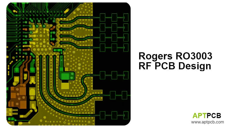
Most RF circuit boards have one thing in common: the substrate's dielectric properties are baked into every transmission line calculation on the board. Change the substrate, and every trace width, every via transition model, every antenna element dimension changes with it. This is why substrate selection happens at the beginning of an RF PCB program, not at the end—and why Rogers RO3003's specific combination of properties has made it the dominant material choice across frequency bands from 24GHz to 94GHz.
This guide is a practical RF design reference for engineers working with RO3003: how the material's properties translate into transmission line geometry across frequency bands, how to launch RF signals onto the board reliably, and what assembly decisions affect the RF performance of a completed module.
RO3003 as an RF Design Platform: The Numbers That Matter
Before routing a single trace, an RF PCB designer working with RO3003 needs three numbers:
Dk = 3.00 ± 0.04. The dielectric constant determines the guided wavelength at any frequency: λ_guided = λ₀ / √Dk. At 77GHz in free space, λ₀ ≈ 3.9mm. On RO3003 (√3.00 ≈ 1.732), the guided wavelength is approximately 2.25mm. Every quarter-wave stub, half-wave resonator, and Wilkinson divider arm is sized from this number. The ±0.04 tolerance means that across production lots, a quarter-wave section designed for 2.25mm will land between 2.22mm and 2.28mm—tight enough that antenna simulation results transfer reliably to hardware.
Df = 0.0010. The dissipation factor sets the dielectric loss per unit length, which flows directly into the link budget. At 77GHz, RO3003's Df produces approximately 0.31 dB/inch of dielectric insertion loss. This number is additive with conductor loss—so total substrate loss on a completed RF PCB is the sum of both contributions, both of which must be within budget before any component or connector losses are added.
TcDk = −3 ppm/°C. The thermal coefficient of Dk determines how much the guided wavelength changes with temperature. At −3 ppm/°C over a 125°C automotive temperature range (−40°C to +85°C), the guided wavelength on RO3003 changes by less than 0.04%. Phased-array beam-steering accuracy across this temperature range requires no active compensation. The material properties of Rogers RO3003 cover these values in full engineering context.
Transmission Line Geometry: From Frequency to Trace Dimensions
The first practical task on any RO3003 RF PCB layout is sizing the controlled-impedance transmission lines. The geometry depends on: Dk, core thickness, copper weight, and whether the structure is microstrip or stripline.
50Ω Microstrip on Standard Core Thicknesses
Approximate 50Ω microstrip trace widths for RO3003 (Dk = 3.00, 1 oz copper, standard formulas as a starting point—use a full-wave EM solver or Rogers MWI-2000 for final values):
| Core Thickness | ~50Ω Trace Width | Primary Application |
|---|---|---|
| 5 mil (0.127mm) | ~4–5 mil | Dense phased arrays with tight element pitch |
| 10 mil (0.254mm) | ~9–11 mil | General mmWave RF layers; most manufacturable |
| 20 mil (0.508mm) | ~18–22 mil | Power handling, lower mmWave bands |
The 10 mil core is the most commonly specified for commercial RF PCB programs. Its ~10 mil trace width is practical to etch to ±10% tolerance using LDI imaging, inspect under 3D AOI, and troubleshoot during prototype evaluation. Thinner cores produce narrower traces that require more precise fabrication control and higher-resolution inspection.
Why Microstrip Is Preferred for RF Layers
Outer-layer microstrip is the dominant transmission line topology for RO3003 RF PCBs for a practical reason: the trace is accessible. It can be probed with a ground-signal-ground (GSG) probe for on-wafer or on-board characterization, inspected by 3D AOI for trace width accuracy, and repaired with focused ion beam or mechanical trimming during prototype debugging.
For RF structures where radiation loss or EMI containment matters, buried stripline (trace between two reference planes) reduces radiation loss at the cost of accessibility. Via transitions from outer microstrip to buried stripline require careful modeling—the stub below the last connected layer creates a quarter-wave resonance at a frequency determined by stub length, and that resonance can fall within the operating band on mmWave designs.
Differential Pair Routing for Modern RFICs
Many current-generation RFICs for radar and 5G applications use differential RF architectures. For a 100Ω differential pair on 10 mil RO3003 (1 oz copper), the individual traces are approximately 8–9 mil wide with 5–6 mil edge-to-edge spacing. Both traces must be equal length within the dielectric wavelength at the operating frequency, and the reference plane beneath the pair must be continuous—no splits or cutouts within several trace widths of the pair.
Surface Finish Selection for RF PCBs: The Performance Argument
At RF and mmWave frequencies, the surface finish on the outer copper layers is not a cosmetic choice—it is part of the RF signal path. The skin effect at 77GHz concentrates current in the outermost ~0.24 μm of the conductor. Whatever material exists in that layer contributes to the effective conductor resistance.
Immersion Silver (ImAg): A 0.1–0.2 μm silver deposit is effectively transparent to RF current at GHz frequencies. The RF signal rides on the underlying copper surface with its actual roughness characteristics intact. ImAg is the standard surface finish recommendation for any RO3003 RF PCB operating above 20GHz.
ENIG: The 3–5 μm nickel underlayer (μ_r ≈ 600 relative permeability at RF) introduces surface impedance that increases conductor loss by approximately 0.1–0.2 dB/inch at 77GHz compared to ImAg. This is measurable and real—on a 3-inch receive-path feed network, that penalty is up to 0.6 dB added to the noise figure of the first receive chain. For final production on mmWave programs, ImAg is the correct choice.
HASL (Hot Air Solder Leveling): Not suitable for RO3003 RF PCBs. The non-uniform surface topography disrupts controlled-impedance trace profiles, and the thermal shock of the hot-air leveling process is incompatible with PTFE substrates.
ImAg requires handling discipline: tarnishing occurs when exposed to sulfur compounds or fingerprint oils. APTPCB ships all ImAg-finished RO3003 boards in sulfur-free packaging, vacuum-sealed in Moisture Barrier Bags with desiccant and Humidity Indicator Cards. After bag opening, boards must proceed to assembly within 5 working days—a scheduling constraint that the RO3003 PCB assembly process guide addresses in detail, including why nitrogen reflow atmosphere is required to prevent ImAg tarnishing during the reflow cycle.
RF Signal Launch: Connector and Probe Access on RO3003
Getting RF signals onto and off an RO3003 PCB reliably—without introducing reflections that corrupt impedance measurements or mask real design problems—is one of the more practically important RF PCB design skills.
Edge-Launch RF Connectors
Edge-launch SMA or SMPM connectors are the most common RF input/output method for test and evaluation boards. For a correct launch on a 10 mil RO3003 core with 1 oz copper:
- The connector center pin must land on the microstrip trace at the same height as the trace center
- The ground tabs must contact the ground plane without creating inductive gaps
- The cutout geometry at the board edge must be sized to match the connector body—an oversized cutout introduces a capacitive discontinuity that creates an impedance bump visible in TDR and VNA measurements
For 77GHz frequencies, 2.4mm (K-connector) or 1.85mm (V-connector) interfaces are required rather than standard SMA (usable to ~18GHz). The connector-to-trace transition must be modeled in the EM simulator and the surrounding geometry—pin length, ground tab spacing, cutout depth—treated as part of the RF design, not the mechanical design.
CPW (Coplanar Waveguide) for GSG Probe Access
When on-board characterization with GSG probes is planned, Coplanar Waveguide is the standard launch structure. A CPW on 10 mil RO3003 with 50Ω characteristic impedance typically uses a 4–5 mil center conductor and 3–4 mil gaps to the ground planes on either side. The ground conductor must be wide enough to form a continuous reference below the measurement plane—narrow ground fingers produce parasitic resonances above 40–50GHz that distort the S-parameter measurement.
GSG probe pads for 77GHz measurements require pitch compatibility with available probe heads (most commonly 100μm pitch for WR-12 waveguide-interface probes). The Rogers circuit board design guide covers CPW geometry, via transition modeling, and the ground via placement rules that apply at millimeter-wave frequencies.
Hybrid Stackup Architecture for RF PCBs
Most commercial RO3003 RF PCBs are not built entirely from RO3003 laminate. The standard production approach—which reduces raw material cost by 30–45% without affecting outer-layer RF performance—uses RO3003 on the outer RF layers and high-Tg FR-4 on internal routing and power distribution layers.
The architecture looks like this for a 6-layer RF PCB:
| Layer | Material | Purpose |
|---|---|---|
| L1 (top) | RO3003 10 mil | Antenna elements, RF feed lines, RF IC pads |
| Bond film | Low-flow high-Tg prepreg | RO3003/FR-4 adhesive interface |
| L2 | High-Tg FR-4 | Ground reference plane |
| L3 | High-Tg FR-4 | DC power distribution, digital control |
| Bond film | Low-flow high-Tg prepreg | FR-4/RO3003 adhesive interface |
| L4 (bottom) | RO3003 10 mil | RFIC connections, secondary RF structures |
The FR-4 inner layers are electrically distant from the outer RF transmission lines. They don't influence the effective Dk of the outer-layer microstrip, which is determined by the RO3003 core and the air above the trace. The RF performance on L1 and L4 is identical to what it would be on a monolithic RO3003 board.
The fabrication complexity introduced by the hybrid interface—bonding film selection, controlled lamination cooling at ≤2°C per minute, inner-layer copper density management—falls entirely on the fabricator. For engineers, the only design-stage obligation is confirming that FR-4 inner layer copper density meets the ≥75% threshold for bow/twist management, which APTPCB's DFM review verifies as part of the standard Gerber acceptance process.
RF PCB Power Handling: Thermal Management on RO3003
A design consideration that often surfaces late in RF PCB programs: RO3003's thermal conductivity is 0.50 W/m/K. For an RF power amplifier module, this is approximately the thermal conductivity of structural foam relative to what's needed to conduct heat from the RFIC junction to the chassis.
Heat does not spread laterally through RO3003 in any meaningful way. The engineering solution is to route heat vertically through copper—via arrays (POFV) beneath the RFIC thermal pad conduct at ~398 W/m/K, bypassing the dielectric entirely. For an RF IC with a 3×3mm thermal pad, a 3×3 or 4×4 array of 0.3mm POFV vias at 0.6mm pitch reduces thermal resistance from the junction to the back of the board from >200°C/W (through dielectric alone) to approximately 15–25°C/W.
POFV design for RF PCBs requires specifying the via fill material, cap plating planarity (APTPCB target: within ±10 μm of surrounding copper), and coverage (≥50% of thermal pad area). The RO3003 PCB manufacturing guide covers POFV design parameters and the X-ray inspection criteria that validate thermal path integrity after SMT assembly.
RF PCB Verification: TDR and VNA Testing
Before components are mounted, bare RO3003 RF PCBs should be verified with two measurements:
TDR (Time-Domain Reflectometry): A step pulse injected into test coupons on the production panel reveals impedance deviations from target. APTPCB performs TDR testing on every production panel, not just qualification lots. Sample TDR reports showing measured vs. target impedance on controlled-impedance structures should be a standard deliverable from any qualified RO3003 fabricator.
VNA S-parameter measurement (on prototype boards): A Vector Network Analyzer measurement through the actual RF trace—from launch connector to launch connector or GSG probe to probe—validates insertion loss and return loss on the physical board before component placement. Comparing measured S21 to EM simulation reveals whether any systematic fabrication variation (trace width, Dk, surface finish) is affecting insertion loss.
A fabricator's TDR report tells you the board matches the impedance target. A VNA measurement through the actual RF path tells you whether the total insertion loss budget is in the right place. Both measurements together establish the RF baseline for the program before any component-related uncertainty is introduced.
Getting RO3003 RF PCBs Into Production
The supply chain structure for RO3003 RF PCBs differs from standard FR-4 in one critical way: Rogers Corporation is the sole manufacturer of RO3003 laminate, and raw material lead time from order to fabricator is 8–12 weeks. Fabricators who pre-stock common core thicknesses deliver prototypes in 3–4 weeks from Gerber acceptance. Those who order per job extend lead time to 10–14 weeks minimum.
For RF PCB programs spanning NPI prototype through production volume, working with a fabricator who maintains strategic Rogers material inventory is a schedule advantage that compounds as the program iterates. APTPCB maintains pre-purchased stock of 5 mil, 10 mil, and 20 mil RO3003 cores with low-profile copper as a standard inventory position.