
Solderability testing asks whether a defined surface can be wetted by solder under specified conditions. The surface might be a PCB pad, plating inside a hole, or a component termination. A useful result identifies that specimen, the test conditions and the agreed acceptance criteria—not just a “pass” label.
For procurement and engineering teams, the first decision is what needs to be evaluated. A component solderability report is evidence about the tested component terminations; it is not a test of the PCB pads they will be soldered to. Likewise, an edge-dip result for a board sample does not necessarily describe solderability inside plated holes.
A passing test can support a release decision within its stated scope. It does not, by itself, demonstrate the quality of every assembled joint or establish long-term product reliability.
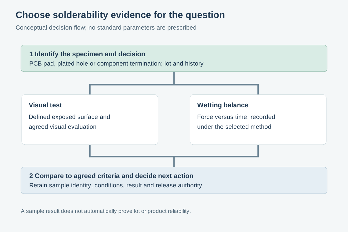
Start with the surface and the decision
Before selecting a method, describe the surface of concern and the decision the result must support:
- Bare-board surface: Identify the pad, exposed finish or other board feature, the fabrication lot and its storage history.
- Plated hole: Identify the hole or hole population and whether the question concerns its internal plating. A test of an exposed board edge is not automatically evidence for the hole wall.
- Component termination: Identify the component part, package or lead style, manufacturer lot, and prior handling or conditioning.
- Assembly process: Identify the board, components, materials and process to be represented. A process trial evaluates their interaction, rather than isolating a single surface.
The distinction matters because the surface finish, exposed geometry and prior history can change the outcome. A result for one component package, board feature or lot should not be assumed to apply to another without an agreed basis.
IPC’s J-STD-002, Solderability Tests for Component Leads, Terminations, Lugs, Terminals and Wires, addresses component-related specimens. IPC’s J-STD-003, Solderability Tests for Printed Boards, addresses printed boards. Specify the applicable document, revision and method in the purchase or quality agreement; do not rely on a standard number alone to settle every sampling or release question.
Choose the method for the question
| Approach | What the result describes | Useful when | Conditions and limits |
|---|---|---|---|
| Visual dip-and-look | The appearance of the defined surface after the prescribed preparation, fluxing and solder exposure | A defined board feature or termination needs to be assessed against visual acceptance criteria | The agreed method must specify what area to examine and how to judge it, including any relevant coverage and defect criteria. Appearance is an evaluated result, not an absence of criteria. |
| Wetting balance | A force-versus-time response as the defined specimen interacts with molten solder | A measured wetting response is needed under controlled conditions | Geometry, solder, flux, immersion setup and timing affect the curve. A curve is not automatically a pass or fail; acceptance limits must be agreed. |
| Process simulation or assembly trial | The observed outcome when selected boards, components and materials undergo a defined process | The concern is how the chosen surfaces behave together in a representative assembly process | It can expose interactions that a separate specimen test misses, but the outcome may not isolate the cause. Inspection and acceptance criteria must still be defined. |
These approaches answer related but different questions. Use one or more according to the decision, not simply because a report happens to be available.
Visual dip-and-look: specify what “acceptable” means
In a visual test, the specimen is exposed to solder under the selected procedure and then examined against the applicable criteria. The report should distinguish what was observed from whether the observation met the agreed requirement.
For example, a report may describe the relevant surface area and observed solder coverage or defects, then record the disposition against the specified method. The applicable criteria depend on the specimen and agreement; there is no useful universal coverage value to substitute for them.
Visual assessment also has limits. An image of an untreated pad or termination can help identify contamination, damage or finish appearance, but it cannot by itself guarantee that the surface will wet. A post-test photograph can document what was seen, but its value depends on identifying the specimen, viewed area and criteria used.
Wetting balance: measured does not mean self-accepting
A wetting balance records a force response over time as a specimen contacts molten solder. The curve can help describe the development of wetting under the test conditions. Depending on the procedure and agreement, the report may include the curve and defined values derived from it.
Those measurements need context. A small termination and a broad PCB feature do not present the same geometry. Different fluxes, alloys, specimen preparation, immersion arrangements or timing can also change the response. Instrument setup, any corrections required by the method, and the reported reference points matter when comparing curves.
The National Physical Laboratory’s Measurement Good Practice Guide 66, Issue 2 discusses solderability measurement and wetting force over time. Its examples and conditions are useful for understanding the technique; they are not automatic acceptance limits for every specimen. Agree on the method and limits before testing, including what will happen if the result falls outside them.
Process simulation: test the interaction you care about
An agreed process simulation can be useful when separate board and component evidence does not resolve an assembly concern. For example, a trial might combine representative boards, components, solder material and flux in a defined process, then inspect selected joints against agreed criteria.
The trial should record which materials and process settings were used, how specimens were selected, and what differences remain from the intended production process. If the trial shows poor results, the board finish, component termination, solder material, process or their interaction may all need investigation. Do not assign the cause from the trial outcome alone.
An assembly trial is also not a substitute for defining the bare-board or component test when either is contractually required. Solder paste inspection and automated optical inspection address different stages of assembly; see when to run SPI and AOI in PCBA.
Internal holes need their own test question
A plated through-hole creates a specific evidence challenge: the surface of interest may be inside the board rather than on an exposed pad or edge. State whether the concern is the pad, the hole wall, or both, and select a specimen and method that address that location.
IPC’s TM-650 2.4.12, Revision A, 1991, Solderability, Edge Dip Method is an older method for an edge-dip evaluation. Its own scope cautions that the result does not necessarily represent the solderability of internal hole plating. It should not be treated as a current universal hole-test procedure or used to infer a hole result from an edge result.
For a through-hole process concern, also consider whether a representative assembly trial is needed to examine the combined effect of the board, termination and process. The practical context is discussed in through-hole soldering basics.
What a useful report should transfer
Ask the test requester, laboratory and release authority to agree on the following before samples are consumed. The final report should retain enough of this information to interpret the result later.
| Item | What to record or resolve |
|---|---|
| Specimen identity | PCB part and revision, feature or hole location, or component part and termination; finish where known; unique sample identifiers. |
| Lot and selection | Manufacturing lot, quantity represented, sample-selection approach and any known reason the samples may not represent the lot. |
| History | Relevant receipt and storage information, handling, prior processing and conditioning, including any treatment specified before the test. |
| Method | Document and contracted revision, procedure, specimen orientation and preparation, plus the defined test conditions. |
| Materials and setup | Solder alloy, flux, equipment setup, timing and other conditions required by the selected method. |
| Acceptance | Criteria agreed before testing, including the surface or measurement to be judged and who can authorize disposition. |
| Result | Visual observations and disposition, or measured values and curves as applicable; deviations, inconclusive observations and the report date. |
| Next action | Release, hold, investigation, additional testing or another approved disposition, with an owner. |
STMicroelectronics’ AN2036, Solderability Tests is useful as an example of solderability testing in a particular product context. Its conditions and criteria should not be copied into an unrelated board or component agreement without confirming applicability.
The sample is not the lot
A report describes the samples actually tested. Whether it supports a decision on a larger lot depends on the agreed sampling plan, how specimens were selected and whether their condition represents the material to be released.
A board coupon, for example, may be convenient to test, but its relevance to a particular pad or hole needs to be established. A component sample from a different manufacturer lot or storage history may not answer the present question. Preserve the connection between samples, packaging and the represented inventory; PCB traceability and lot control provides related guidance.
Solder exposure and preparation can alter or consume a specimen. Keep tested items segregated and do not return them to assembly as normal stock unless an authorized disposition permits it. If the only available item is an intact production board, agree in advance whether testing would damage or contaminate features needed for assembly. Reserve representative samples where possible.

Hypothetical conflict: a component report arrives, but the concern is a PCB pad
Invented example: A buyer receives a component solderability report marked “pass.” The assembly engineer is concerned about wetting on a PCB pad from the boards awaiting assembly. No actual pad test result is available in this example.
The report is not contradictory, and it does not establish that either item failed. It addresses a different specimen: the component termination rather than the board pad.
The team should first request or confirm:
- Report and sample identity: Which component part, termination and samples were tested? What PCB part, revision and pad are in question?
- Date and lot: When was the component tested, and does its lot match the material to be assembled? Which board lot is affected?
- Prior conditioning and history: How were the tested components and the boards stored, handled or otherwise conditioned?
- Method and acceptance: What procedure, conditions and criteria produced the component disposition? What method and criteria would address the pad?
- Next action and authority: Who decides whether to hold the board lot, request representative pad testing, run a process trial or proceed under an approved disposition?
If the component report lacks key identifiers or conditions, request clarification rather than treating its pass label as complete evidence. If a pad test is commissioned, define its specimen and acceptance before testing. If both separate tests pass but a representative assembly trial has an unfavorable result, investigate the combined materials and process rather than declaring either report invalid.
Handle exceptions without turning a retest into rework
An inconclusive observation, a missing condition or a result outside the agreed criteria calls for a documented decision—not an automatic repeat until a favorable result appears.
- Hold the affected material as appropriate. Identify the potentially affected lot and prevent unapproved release while the discrepancy is assessed.
- Check validity first. Confirm specimen identity, method, equipment status, setup, conditioning, observations and any deviations. A documented test error may justify an agreed repeat.
- Keep retesting distinct from rework. Retesting may assess additional, previously untested or, where the method permits, previously tested samples under an agreed plan; the sample history must be recorded. Rework or surface treatment changes the material; testing after that change evaluates the treated condition, not necessarily the original lot condition.
- Agree on representation again. If material is treated, define which items received the treatment, how they will be identified and what samples represent them. Do not extend a result to untreated or differently handled stock without justification.
- Record the disposition. The designated release authority should approve the evidence and next action under the contract or quality system.
Cleaning can be relevant to an assembly investigation, but it is not a substitute for an agreed solderability test or an authorized recovery process. For the separate issue of assembly residues, see cleaning after soldering.
A practical handoff to APTPCB
For a project discussion, include the board or component identity, affected lot, feature of concern, available reports, intended assembly process and the standard revision and acceptance requirements you want applied. Identify any missing information as unresolved rather than assuming a default method.
Use request a quote for a project inquiry or contact APTPCB to discuss the required documentation and next steps. Confirm the testing arrangements and responsibilities explicitly; do not assume a particular test or report is included.
Public reference documents
- IPC, J-STD-002, Solderability Tests for Component Leads, Terminations, Lugs, Terminals and Wires — component-related scope; use the revision agreed in the contract.
- IPC, J-STD-003, Solderability Tests for Printed Boards — printed-board scope; use the revision agreed in the contract.
- IPC, TM-650 2.4.12, Revision A, 1991, Solderability, Edge Dip Method — older edge-dip method; not necessarily representative of internal hole plating.
- National Physical Laboratory, Measurement Good Practice Guide 66, Issue 2 — wetting-force measurement context; its examples are not universal acceptance criteria.
- STMicroelectronics, AN2036, Solderability Tests — product-specific test context; its conditions should not be generalized without checking applicability.