
Via stitching uses plated vias to connect selected copper areas on different PCB layers, often on the same ground net. A designer may use those connections to join ground pours, provide a nearby return-current path where a signal changes reference planes, or form part of a via fence around an RF structure. The right placement depends on which of those jobs the vias are supposed to do.
Start with the signal path and its reference planes, not a fixed grid copied over the whole board. Identify the layers and nets being joined, check the route that current can take, and then confirm the via geometry with the fabricator. A dense pattern cannot restore a missing reference plane, prove an EMC result or safely connect unrelated voltage domains.
For the basic construction of plated holes, see what a PCB via is. For the larger layer-order decision, see PCB stackup design. The discussion here focuses on how a stitching connection is used and what must be reviewed around it.
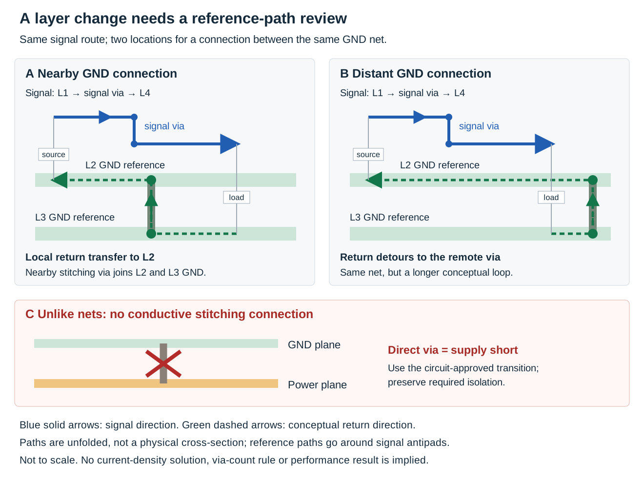
The non-scale, unfolded net-and-layer path diagram compares the same signal layer change with a nearby GND connection and a distant GND connection. Solid blue arrows show signal direction; dashed green arrows show a conceptual return route on the two same-net reference planes and through their connecting via. Plane paths pass around the signal via's antipads; the drawing unfolds those paths for clarity. The lower view preserves the unlike-net counterexample: a conductive via between GND and a power plane would short the supply. These conceptual circuit paths are not a current-density solution, fabrication geometry, required via count or proof of electrical performance.

Real photograph of an unpopulated circuit board with visible holes, traces and pads. The layer connections and electrical roles of the holes cannot be established from this view. Photo: Vishnu Mohanan / Unsplash.
What is a stitching via?
A stitching via is defined by its purpose in a layout, not by a unique hole shape. It connects copper features across layers so that they have a deliberate electrical relationship. A common example is a plated through-via joining top and bottom ground pours to an internal ground plane. Blind or buried structures may also be used where supported and appropriate, but their layer span, fabrication sequence and cost must be reviewed for the actual board.
A signal via carries a signal from one layer to another. A stitching via in this discussion connects the relevant reference copper. Both may be near the same transition, but they are not interchangeable: connecting the signal net to ground would change the circuit. A thermal via is selected for a thermal path, while a power via carries current between power features. A via may have more than one role, but each role still needs its own electrical, thermal and manufacturing review.
Ground copper on two layers is not automatically connected merely because both areas look green in the CAD viewer or carry the same net label. Inspect the actual plated layer span and copper connections after zones are refilled. Conversely, two adjacent copper areas should not be joined simply because their names both include “ground.” Their intended electrical relationship, isolation requirements and current paths are design decisions.
Why does a signal layer change deserve attention?
A signal and its return current form a circuit. At high frequencies, the return-current distribution is strongly influenced by the nearby reference structure and the geometry around the route. When a signal changes layers, its closest reference can change too. If the two reference structures are on the same net but occupy different layers, a nearby connection between them can provide a local path for the return current rather than forcing that current to rely on a more distant connection.
That does not mean every signal via needs the same number of ground vias. First identify the actual outgoing and incoming reference planes, the signal's edge rate or frequency content, the local geometry and the system's performance targets. If both trace sections retain a suitable common reference plane, the return-path question differs from a transition between two separate planes. The via, antipads, reference geometry and nearby connections can still affect the complete transition and may need analysis.
Texas Instruments' AM65x/DRA80xM DDR Board Design and Layout Guidelines gives a concrete, device-specific example: it prefers retaining the same reference plane when possible and discusses nearby stitching connections where the reference changes between planes on the same net. Its guidance is for the specified DDR designs; the correct arrangement for another interface must be evaluated against that interface and stackup.
What if the reference changes from ground to power?
Do not place a conductive via between ground and a power plane to imitate a ground-to-ground stitching connection. That would create an unintended DC short. A change between unlike reference nets needs a circuit-specific return-path strategy. In the TI DDR example, nearby bypass capacitors provide an alternative connection between ground and the specified supply references. The selected component, its mounting, the surrounding plane geometry and its impedance over the relevant frequencies all matter.
This is not permission to bridge an isolation barrier or arbitrarily connect separate grounds with a capacitor. Safety, creepage, leakage, noise and system architecture requirements may restrict any connection. The circuit owner and applicable safety requirements determine what is allowed; a layout rule or an automatic stitching command cannot make that decision.
Four situations that need different reviews
| Layout situation | First question | Candidate action | What still needs verification |
|---|---|---|---|
| A trace changes layers but keeps an appropriate common reference. | Does the reference remain continuous around the transition? | Review the signal via, antipads and surrounding reference geometry. | Transition discontinuity, actual field distribution and interface limits. |
| A trace changes between two reference planes on the same ground net. | Are both planes genuinely on the intended net and connected across the relevant layers? | Consider a nearby ground stitching connection where it supports the return path. | Layer span, clearance, placement, other paths and the actual performance target. |
| A trace changes between a ground reference and a power reference. | What connection between the unlike references is permitted by the circuit? | Consider the approved bypass or reference-transition strategy for that circuit. | DC isolation, frequency-dependent impedance, component mounting and system validation. |
| An RF route has grounded copper beside it. | Is the geometry a designed transmission-line structure, and where does its return flow? | Evaluate ground connections or a via fence as part of the complete RF layout. | Impedance, field behavior, coupling, losses and relevant RF measurements. |
This table is a review aid, not an instruction to add a particular number of holes. A shared net name alone does not establish that each copper region has the intended connection after manufacturing output generation. Examine the actual plane shapes, clearances and via span.
What is a via fence?
A via fence is a row or pattern of vias used with copper regions to influence the electromagnetic boundary of a layout. For example, a grounded coplanar waveguide has a signal conductor with adjacent ground copper and a reference plane; a fence can connect the adjacent ground to the reference as part of that structure. Analog Devices illustrates ground via fences beside a coplanar waveguide in its PCBs Layout Guidelines for RF & Mixed-Signal. NXP's IW416 Design Guide likewise shows ground-pour stitching for its particular RF design.
A fence is not a solid metal wall. Fields can extend through openings and around the structure, and the result depends on the route, stackup, nearby metal, via dimensions, spacing, terminations and frequency range. A fence on the board edge is not automatically equivalent to a properly connected shielding enclosure. Use a layout, simulation or measurement approach suited to the actual isolation and emissions question.
You may encounter spacing rules expressed as a fraction of wavelength or a fixed distance. Treat those as starting assumptions for a specified geometry, not universal acceptance limits. An RF component vendor's spacing for one shield or evaluation board does not establish a safe spacing for another product. Also consider practical gaps: connectors, mechanical cutouts, mounting holes and changes in the reference copper can interrupt an otherwise regular row.
A wavelength estimate is not a fence specification
For a simple microstrip approximation, the guided wavelength can be estimated as λg ≈ c / (f × √εeff), where c is the speed of light, f is frequency and εeff describes the effective permittivity of that particular propagation structure. NXP's High frequency design considerations, AN12298, discusses why the effective value of a microstrip depends on both the substrate and surrounding air. It is not necessarily the bulk dielectric constant printed on a laminate datasheet.
For illustration only, take f = 2.5 GHz, an assumed εeff = 3.0, and c ≈ 300 mm/ns. The free-space wavelength is about 120 mm, while the estimated guided wavelength is 120 / √3 ≈ 69 mm. These are hypothetical inputs, not measurements of a board. They show why using free-space wavelength alone can mislead; this example does not produce a design pitch, shielding level or compliance result.
Choose candidate spacing in three steps:
- Set the evaluation bandwidth. Use the actual interface's edge rates and operating bands; the clock fundamental alone may omit relevant fast-edge content.
- Fix the structure. Identify the stackup, copper boundaries and relevant propagation mode. A plane cavity or enclosure may differ from the trace's microstrip mode. Prefer the applicable component reference-layout geometry within its stated conditions.
- Validate the complete candidate. Review pitch, distance from the route or board edge, and openings together using an appropriate electromagnetic model or measurement against the project's targets. Check fabrication clearances and drill constraints as part of the same review.
Before and after an automated via pattern
- Identify the intended net, layer span and copper regions that must be connected. Confirm which voltage domains and isolation boundaries must stay separate.
- Choose a fabrication-compatible via template and the area or row the pattern may occupy. Record the intended purpose: local return, plane connection or an RF boundary.
- After placement, refill copper and inspect each affected layer. Check the actual pad/plane contacts and examine nonconnecting-layer antipads for slots, narrowed reference copper or damaged isolation clearance.
- Run the relevant connectivity, spacing and drill checks, then review the plotted copper and drill data. Remove or investigate unconnected vias; a visible grid is not proof of a useful connection.
- Preserve the approved pattern and settings with the design revision. If automatic regeneration changes the geometry, repeat the checks that depend on it.
The commands and rule hierarchy vary by CAD product and version. The checks above define what to verify; they do not assume that a particular tool automatically selects the correct net, layers or return path.
Does more stitching always improve the board?
No. Adding vias can connect useful copper regions, but each hole also occupies routing area and changes nearby copper clearances. An unintended clearance around a via can narrow a reference plane or alter a controlled-impedance structure. Closely placed holes, small annular rings, board-edge clearance and the chosen drill process affect manufacturability. The design team should evaluate the complete pattern after CAD clearances and manufacturing rules are applied.
A regular ground grid may help connect large pours, but it does not replace a local review of a critical layer change. Likewise, placing vias along a plane split does not automatically create a continuous return directly underneath a trace that crosses the gap. Where practical, preserve a continuous reference or change the route or stackup; if a discontinuity cannot be avoided, assess the allowed return path and its system impact explicitly.
Do not use a stitching pattern as a substitute for component decoupling, a protective-earth connection, thermal analysis, shielding design or final EMC testing. Those tasks may interact with ground connections, but they have different requirements and must be evaluated in their own context.
A hypothetical four-layer review
Suppose a designer routes a fast digital signal on the top layer, with an internal ground plane as its reference. The signal then moves to the bottom layer, where a different internal ground plane provides the intended reference. Both planes belong to the same approved ground net. The team is concerned about the transition, but the first layout has no local connection between the two planes near the signal via.
The team can work through the decision in order:
- Confirm the actual stackup: identify both reference layers and verify that the signal route has suitable nearby reference copper on each side of the transition.
- Verify that the two reference planes really are intended to be connected on the same net. Check whether any isolation, partitioning or controlled return-current requirement changes that decision.
- Evaluate a nearby ground stitching via with a layer span that connects those planes. Check the signal and ground clearances, antipads and the space needed for reliable fabrication.
- Inspect the resulting copper and drill outputs after the design rules and pours have been regenerated. A nominally correct symbol is not enough if an unexpected clearance isolates the intended copper. If the connection is missing, verify the assigned net and layer span, inspect pad removal, plane clearances and zone settings, correct the approved design, then refill the zones and repeat connectivity and manufacturing-output checks.
- Assess the transition against the interface's signal-integrity and EMC plan. Depending on the product, this may involve review, simulation, measurement or a combination; a layout illustration is not a test result.
If one reference plane is changed to a supply net instead, replace the third step with the circuit-approved reference-transition strategy described above. This example is hypothetical; it does not describe a customer design or guarantee compliance.
How do fabrication and assembly choices affect stitching vias?
Provide the fabricator with the stackup and drill data so that the via can actually connect the intended layers. Specify plated or non-plated features accurately, identify through, blind or buried spans when used, and review finished hole sizes and tolerances under the project's fabrication rules. Dense stitching can increase drill count and may affect panel utilization or cost, but the effect depends on the order and manufacturing process; request a project-specific assessment rather than assuming a fixed surcharge.
Check copper-to-hole spacing, annular ring, clearances in neighboring planes and distance from the finished board edge. Ask the fabricator to assess drill registration and finished-hole tolerances against the rings and clearances on affected layers; the allowable values depend on the construction and process. A ground via passing through a power layer needs the specified clearance from that layer. Likewise, if a via is meant to connect a particular ground plane, confirm that the pad and plane connection are not removed by a clearance or fabrication setting. The electrical netlist and the plotted copper should tell the same story.
Surface treatment matters as well. An open via, a tented via, a plugged via and a filled or capped structure are different manufacturing choices. When a stitching via is near solderable pads, assembly review should consider solder mask openings and the intended process. Do not assume that a mask-covered via is filled or sealed, or that every via near a component needs the same treatment. Where a via is placed in a component pad, the project may require additional filling and planarization decisions; see via-in-pad manufacturing for that separate topic.
Compare a proposed stitching change
Where performance is important, compare the original and proposed layout using a plan agreed by the design team. For example, two representative test structures might use the same stackup, signal route, connector launch and measurement setup, with the intended local stitching arrangement as the documented change. Inspect the manufactured geometry and identify board revisions before drawing conclusions.
Choose a measurement suited to the question: a calibrated TDR or network-analyzer measurement can help compare a specified transition or channel, while radiated-emissions work requires an appropriate system and test setup. Keep fixtures, reference planes, calibration, frequency range and acceptance limits consistent where a direct comparison is intended. Include manufacturing variation in the plan if the decision depends on repeatability. No result is implied by this hypothetical comparison, and passing a coupon measurement alone does not establish product-level EMC compliance.
What should be sent for review?
Include the current fabrication package, netlist, stackup, drill and layer-span information, controlled-impedance requirements and a drawing identifying the relevant routes, reference planes and any intended fence or stitching pattern. Note which copper areas are allowed to connect, which domains must remain separate, and whether the design team is requesting a manufacturing check, an impedance calculation or a broader signal-integrity review. These are different scopes.
For a project-specific discussion, request a quote or contact the team. Agree the fabrication options and deliverables for the actual construction. The fabricator can review buildability and the information supplied; the product's design authority remains responsible for the circuit, isolation decisions and system-level qualification.
Common questions
Are stitching vias needed on a two-layer PCB?
They can be useful when selected copper areas on the two sides need a deliberate electrical connection. Whether a particular layout needs them, and where, depends on the signal paths, copper geometry, assembly constraints and performance requirements. A two-layer board with extra vias still needs usable return paths and adequate plane continuity.
Can a stitching via carry high current?
A plated via can conduct current, but the current capability of a particular structure depends on its geometry, plating, temperature rise, current distribution and surrounding copper. A nominal hole size or a generic number of stitching vias is not enough to establish a safe current rating. Analyze the actual connection and applicable operating conditions.
Does a via fence guarantee lower EMI?
No. A properly designed and connected fence can be one part of an RF or EMC strategy, but its effect depends on the complete structure and frequency range. Evaluate the board together with its components, connectors, cables, enclosure and test conditions.
References
- Texas Instruments, AM65x/DRA80xM DDR Board Design and Layout Guidelines, SPRACI2A, revised March 2019: reference-plane transitions for the specified DDR interfaces.
- Analog Devices, PCBs Layout Guidelines for RF & Mixed-Signal, 2011: grounded coplanar waveguide and via-fence examples.
- NXP Semiconductors, IW416 Design Guide, AN13125, Revision 1, 26 May 2021: product-specific RF ground-pour and stitching examples.
- NXP Semiconductors, High frequency design considerations, AN12298, December 2018: microstrip effective permittivity and guided-wavelength context.