
A via in a PCB is a small plated hole that connects copper on one layer to copper on another. A circuit board via is sometimes just called a via hole. The hole is drilled, its wall is coated with copper, and the resulting barrel carries a signal, power, or ground from one layer to the next. Vias are what make a multilayer circuit board possible: without them, every trace would have to stay on the layer where it started.
Most boards only need plain through-hole vias. Blind, buried, micro, and via-in-pad structures exist to solve specific density problems, and each one adds drilling, lamination, or plating steps that you pay for. The useful question is not "which via is best" but "what is the cheapest via structure that still lets this layout route?"
This guide explains what vias are, the main types of vias, how via size and aspect ratio limit your choices, and how to call vias out so the fabricator quotes the board you designed.
Key takeaways
- A PCB via is a plated hole that joins copper on two or more layers. A component hole holds a lead; a via only carries current between layers.
- Through vias are the default and the cheapest. Blind, buried, and microvias trade cost for routing space.
- Aspect ratio (board thickness divided by drilled hole diameter) sets the smallest through via you can plate reliably on a given board thickness.
- Every additional lamination cycle, laser step, or fill-and-cap operation shows up in price and lead time. Count them before you commit to a structure.
- Put vias on the fabrication drawing as a drill table by layer pair, with fill, cap, and protection requirements stated, rather than leaving them to CAM interpretation.
What is a via in a PCB?
The word comes from the Latin for "path", and some engineers expand it as vertical interconnect access. On a circuit board, a via has three parts:
| Part | What it is | Why it matters |
|---|---|---|
| Barrel | The plated copper wall inside the drilled hole | Carries the current; its plating thickness and integrity decide reliability |
| Pad (land) | The copper ring around the hole on each connected layer | Gives the drill a target and the barrel a place to join the trace |
| Antipad (clearance) | The copper-free gap around the barrel on planes it must not touch | Prevents shorts to planes it passes through and affects impedance |
The ring of copper left between the hole edge and the pad edge is the annular ring. If the drill lands off-center, the ring thins out on one side, which is why drill registration matters as much as hole size.
Vias versus through-holes for components
Both are plated holes, and on a drill file they look alike. The difference is what goes in them. A component hole is sized for a lead or press-fit pin, so its finished diameter and tolerance are set by the part. A via carries no lead, so it can be much smaller, and its job is purely electrical or thermal. Some boards also use non-plated holes for mounting, which are neither.
Which via type does your BGA need: through, blind, micro, or via-in-pad?
There are four basic via types, plus a few variants built from them. The table summarizes how APT's drilling page describes each structure and how it is produced.
| Via type | What it connects | How it is made | Typical reason to use it |
|---|---|---|---|
| Through via (PTH) | Top layer to bottom layer, passing every layer | Mechanical CNC drilling after the final lamination | Standard signal and power routing |
| Blind via | An outer layer to one or more inner layers, not through the board | Mechanical controlled-depth or laser drilling | Fan-out from dense parts, recovering routing space on other layers |
| Buried via | Inner layers only; invisible from the outside | Mechanical drilling on an inner sub-lamination | Crossing dense inner routing channels |
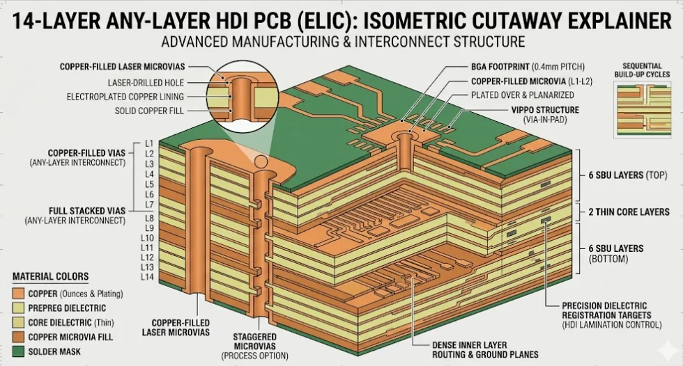
| Microvia | One build-up layer to the next | Laser ablation on a thin dielectric | HDI structures and fine-pitch BGA escape |
| Stacked microvia | Several microvias directly on top of one another | Laser ablation with each lower via filled and plated flat | The densest routing, very fine BGA pitch |
| Staggered microvia | Microvias offset from layer to layer | Laser ablation | Density with less stacking, often preferred for thermal cycling |
| Via-in-pad (VIPPO) | A via placed inside an SMD pad, filled and plated over | Drilling plus fill, planarization, and cap plating | Fine-pitch BGA breakout without dog-bone traces |
| Backdrilled via | A through via with the unused copper stub drilled away | Controlled-depth counter-drilling | Reducing stub reflections on fast serial links |
| Thermal via array | A grid of plated holes under a thermal pad | Mechanical drilling | Moving heat from a power device into planes |
Through vias, blind vias, and buried vias are the core vocabulary. Microvias and via-in-pad are where HDI begins. For how blind and buried spans are planned layer by layer, see the blind and buried via planning guide.
Most via guides list 4 via types and stop. This section adds the 0.4 mm pitch BGA trigger for switching types, and what stays the same at 0.65 mm or larger.
Through vias
A through via is drilled after all layers are laminated, so it costs one drilling and one plating pass. It passes every layer, which means it also blocks routing on every layer, even the ones it does not need to connect. On a board with two or three dense packages, that blocking is usually what pushes a design toward blind or buried vias.
Blind and buried vias
A blind via starts on an outer layer and stops inside the board. A buried via starts and stops inside. Buried vias are drilled and plated on an inner core or sub-stack before it is laminated with the rest of the board, so each buried span normally adds a lamination cycle. Blind vias can be made by controlled-depth mechanical drilling or by laser, depending on depth and diameter.
Microvias
A microvia is a small laser-drilled via that spans a single thin dielectric layer. On APT's drilling capability matrix, CO2 laser microvias reach 0.10 mm and UV laser microvias reach 0.075 mm, with a 1:1 aspect ratio per build-up layer. Microvias are the building block of HDI notation such as 1+N+1 (one build-up layer on each side of a core) and 2+N+2 (two build-up layers per side).
Via drill and aspect ratio: what limits the smallest via you can actually order?
Via size is limited by two things: how small a hole the factory can drill, and how deep a hole of that size can be plated evenly.
Aspect ratio is the board thickness divided by the drilled hole diameter. A 1.6 mm board with a 0.15 mm drill has an aspect ratio of about 10.7:1. Plating solution has to flow through the full length of the barrel, so a deeper, narrower hole is harder to plate to a uniform copper thickness.
These are the figures APT publishes on its PCB drilling capability page:
| Parameter | Mechanical CNC drilling | CO2 laser | UV laser |
|---|---|---|---|
| Minimum diameter | 0.15 mm (6 mil) | 0.10 mm (4 mil) | 0.075 mm (3 mil) |
| Maximum diameter | 6.35 mm (250 mil) | 0.20 mm (8 mil) | 0.15 mm (6 mil) |
| Aspect ratio | 10:1 to 12:1 in standard production; up to 15:1 on validated thick backplanes | 1:1 per build-up layer | 1:1 per build-up layer |
| Hole types | PTH, blind, buried, NPTH, slots | Blind microvia | Blind microvia, direct copper |
Those values are capability limits, not design targets. Combining several limits on one board, such as the smallest drill on the thickest stackup, needs a feasibility review against the actual stackup and panel. If your layout has room for a larger via, using it gives the plating process more margin and usually costs less.
Most guides quote a 10:1 aspect ratio as the rule. This one shows the 12:1 to 15:1 range APT validates on small runs, and why the conservative number is conservative.
How to size a through via
Work from the board, not the drill table:
- Fix the finished board thickness first. It sets the depth every through via has to be plated.
- Divide that thickness by the candidate drill size. If the result sits near the top of the supplier's production range, move up a drill size where routing allows.
- Add the annular ring the fabricator needs around the drill, then check that the pad still fits your pitch.
- If the pad does not fit, that is the point where a blind via, microvia, or via-in-pad becomes worth its cost.
Via-in-pad and filled vias
Via-in-pad places the via inside the component pad instead of beside it. Open holes in a pad would wick solder away from the joint during reflow, so the via is filled, planarized, and plated over. APT's drilling page lists VIPPO for fine-pitch BGA breakout and solder-wicking prevention, and as the base that lets one microvia be stacked on another.
Filling is not only for via-in-pad. Fill may be specified to keep solder mask or flux out of holes, to give a flat surface for assembly, or to support a stacked microvia. Fill material can be conductive or non-conductive, and the choice should be recorded on the drawing. For the process controls and acceptance points, see the via-in-pad manufacturing guide and the article on void control for VIPPO under BGAs.
Via protection (tenting, plugging, or filling with or without a cap) is classified in IPC-4761. Name the protection method you want on the drawing. "Tented" alone leaves room for interpretation.
Choosing a via structure: cost and lamination count
This is the decision table. Start in the top row and move down only when the layout forces you to. Relative cost is a ranking for the same board size and layer count, not a price.
| Via structure | Drilling steps | Extra lamination cycles | Relative cost | Move to it when |
|---|---|---|---|---|
| Through vias only | One mechanical pass | None | Lowest | Default; every net can escape with through vias |
| Through + mechanical blind (controlled depth) | Mechanical plus depth-controlled pass | Usually none | Low to moderate | A few outer-to-inner connections free up a congested layer |
| Through + buried | Mechanical on sub-stack, then final | One per buried span | Moderate | Inner channels are blocked, but outer layers are not |
| 1+N+1 HDI (one microvia layer per side) | Laser plus mechanical | One build-up cycle | Moderate to high | BGA pitch is too fine for through-via fan-out |
| 2+N+2 HDI (staggered or stacked) | Two laser steps per side plus mechanical | Two build-up cycles | High | One microvia layer still does not escape the package |
| Via-in-pad (filled and capped) | Adds fill, planarization, cap plating | None by itself | Adds to any of the above | Dog-bone fan-out does not fit between pads |
| Backdrill | Adds controlled-depth counter-drill | None | Adds to any of the above | Stub length hurts a fast channel |
Two rules keep this table honest:
- Count lamination cycles. Each one adds pressing, drilling registration, and inspection time. APT's HDI pages note that a 2+N+2 build adds lamination, registration, plating, inspection, cost, and schedule compared with 1+N+1.
- Do not mix structures casually. A board with buried vias, stacked microvias, and backdrilling has three separate process risks. If one structure can solve the routing alone, use one.
APT's rigid PCB capability page notes that fine-pitch BGAs around 0.4 mm or 0.5 mm, tight routing channels, or high-speed layer transitions that cannot be achieved with through vias are the usual triggers for an HDI build. When that is your situation, the HDI PCB manufacturing team can review whether a 1+N+1 structure is enough before you design for 2+N+2.
When vias affect signal integrity
At high data rates the via is part of the transmission line. The unused part of a through via below the last connected layer, the stub, can reflect energy. Options are to route the fast signal to a layer near the bottom, use a blind via, or backdrill the stub. APT publishes a backdrill depth accuracy of ±50 μm. The backdrill planning guide covers how to define depth and stub targets.
Thermal vias
Thermal via arrays move heat from an exposed pad into internal planes. They are ordinary through vias in a grid, but they create a solder-wicking problem under bottom-terminated packages. Decide early whether they will be filled, plugged, or left open with a paste-reduction pattern on the stencil.
How vias drive PCB cost
Beyond the structure itself, three via choices move the quote: total drill count (machine time), the smallest mechanical drill (tool wear and drill stack height), and aspect ratio near the top of the supplier's range (slower plating or extra cross-section checks). Microsection coupons for via structures add inspection scope when the order calls for them.
If the quote is higher than expected, ask the fabricator which via feature is driving it. Often one package forced the whole board into HDI, and moving or swapping that part removes a lamination cycle.
Via callouts on the fab drawing
A clear callout is the cheapest way to avoid a wrong build. Include:
- A drill table by layer pair, for example L1–L2 laser, L2–L7 buried, L1–L8 through, with finished or drilled sizes stated and which one is which
- Plated versus non-plated holes, separated in the NC drill files
- Via fill requirement and material (conductive or non-conductive), and whether a cap is required
- Via protection method by IPC-4761 type where used, and on which side
- Via-in-pad locations, if any, and the flatness or dimple expectation for those pads
- Backdrill locations, the layer that must stay connected, and the allowed stub
- The acceptance class for the board, for example IPC-6012 Class 2 or Class 3
APT's HDI capability page asks for the proposed stackup, a layer-to-layer via map, stacked or staggered callouts, buried vias, and via-in-pad locations with the RFQ. Sending those with Gerber X2, ODB++, or IPC-2581 data lets CAM confirm the structure instead of guessing it.
Why involve APTPCB in via planning?
APT reviews via structures as part of the engineering check before fabrication release. The review compares the via map with the stackup, finished thickness, drill sizes, and aspect ratio, then flags combinations that sit at the edge of the HDI capability range or that could be simplified. Final via diameter, aspect ratio, capture pad, and sequential-lamination feasibility are confirmed only after that review, because they depend on the complete material, stackup, panel, and quantity.
Relevant standards and references may include:
- IPC-2221: generic standard on printed board design
- IPC-2226: sectional design standard for HDI printed boards
- IPC-6012: qualification and performance of rigid printed boards
- IPC-4761: design guide for protection of printed board via structures
- IPC-A-600: acceptability of printed boards
Frequently asked questions
What are vias in a PCB used for?
Vias in a PCB carry a signal, power, or ground connection from one copper layer to another through a plated hole. It lets traces change layers, ties planes together, and in arrays it can move heat from a component into internal copper.
What are the main types of vias?
The main types of vias are through vias, blind vias, buried vias, and microvias. Variants built on these include stacked and staggered microvias, via-in-pad (filled and capped), backdrilled vias, and thermal via arrays.
What is the smallest via size a PCB can have?
It depends on how the hole is made. APT publishes 0.15 mm as the minimum mechanical drill, 0.10 mm for CO2 laser microvias, and 0.075 mm for UV laser microvias. The usable size on a specific board also depends on its thickness, stackup, and pad size.
What is the difference between a blind via and a buried via?
A blind via starts on an outer layer and ends on an inner layer, so you can see it from one side. A buried via connects inner layers only and is not visible from either surface. Buried vias usually add a lamination cycle because they are drilled before the final press.
Do vias increase PCB cost?
Through vias add little beyond drill time. Blind, buried, laser, filled, capped, and backdrilled vias each add process steps, and HDI build-up layers add lamination cycles. The structure matters more than the number of holes.
Can you put a via in a pad?
Yes, but an open via in a pad will draw solder away from the joint. For BGA and fine-pitch pads, the via is normally filled, planarized, and plated over (VIPPO) so the pad is flat and solderable.
Via RFQ checklist
- Minimum mechanical drill size required
- Minimum laser drill size and type: CO2 or UV laser
- Aspect ratio (AR) of the deepest through via
- Via type by layer pair: through, blind, buried, microvia, via-in-pad
- Via fill requirement: conductive, non-conductive, or copper overfilled
- Via protection method: tented, plugged, or filled by IPC-4761 type
- Backdrill required: Y/N; target depth and depth tolerance ( ±50 µm)
- Interference-fit press-fit pin hole size and tolerance if applicable
- HDI structure: 1+N+1, 2+N+2, or other sequential lamination
- IPC-6012 acceptance class for the board
- Impedance-controlled nets with target impedance and tolerance
- Backdrill drill table: layer pair, stub length target, allowed residual
Use this when you request a quote from a board house.
Picking the simplest via that routes
Start with through vias and a sensible drill size for your board thickness. Add a structure only when a specific package or channel cannot route without it, and count the lamination cycles each step adds. Then put the result on the drawing as a drill table and a via map. That gives the fabricator what it needs to quote the board you designed, and it gives you a clear place to cut cost if the first quote comes back high.