
Via tenting means covering a via with solder mask on one or both sides of a PCB. It can reduce exposed copper around a via, but a mask-covered opening is not proof that the hole is sealed, filled, watertight or suitable as a flat solderable pad. If the design needs one of those outcomes, specify it separately and agree on how it will be verified.
That distinction matters most where vias sit close to component pads, need to remain accessible for testing, or occupy a soldered pad. The right treatment is a location-specific decision, not a single setting for the entire board.
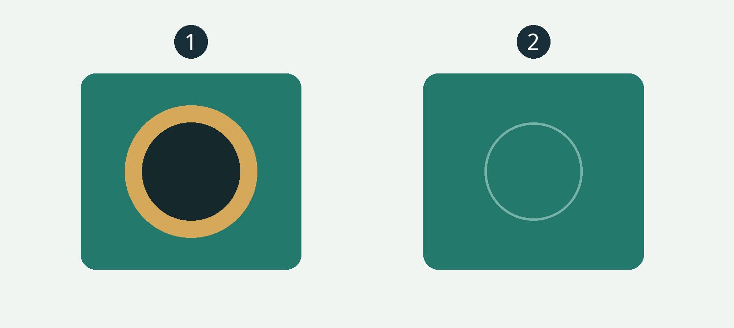
In these conceptual top views, 1 shows an exposed via and 2 shows mask covering the via. They are not to scale; a top view cannot prove that a covered hole is sealed.
What does a tented via actually cover?
The layout specifies where the solder mask is open and where it remains over copper. A tenting setting requests mask coverage over a via. KiCad 9's PCB Editor documentation, for example, treats front and back tenting as separate controls. The finished result still depends on the exported mask data, hole geometry and the fabrication process.
Mask coverage is different from inserting material into the hole. A designer who needs a plugged hole, a filled barrel or a copper-capped surface should state that requirement rather than expect the fabricator to infer it from a mask layer. The public preview of IPC-4761 lists tented, plugged, filled, covered and capped constructions separately and discusses how protection should be specified in procurement documentation. It does not supply a universal acceptance limit for every project.
Which treatment should be specified?
| Design need | Treatment to discuss | What needs confirmation |
|---|---|---|
| Reduce exposed copper around a via | Solder-mask cover on the relevant side | Locations, side, exported mask and the agreed coverage criteria; do not assume the hole is sealed. |
| Access for a test probe or other contact | Mask opening at selected vias | Accessible side, opening and location; confirm the planned test access with the assembly and test teams. |
| Control entry into a via | A separately specified plugging or filling process | Material and extent, sides, inspection and the result required for the application; a mask cover alone does not establish it. |
| Solder onto a pad containing a via | A defined filled, planarized and capped construction where required | Hole locations, finished pad surface, materials and acceptance criteria; review the actual pad and component with the fabricator and assembler. |
These are starting points for a design review, not interchangeable process names or a guarantee that any particular construction is available for every board. The via-in-pad manufacturing article goes deeper into filled and capped solderable pads; PCB via basics explains how vias connect layers.
What changes near a component pad?
Consider a via beside a fine-pitch solder pad. The pad must have the intended mask opening for assembly, while the via may be covered. Review the copper and mask geometry together: a desired separation in the CAD view is useful only if the released mask output and the manufacturing process can produce the intended result. Ask the fabricator to review tight mask features rather than relying on a generic clearance figure.
If a via is inside a soldered pad, the concern is different. An open hole can allow solder to move away from the joint during assembly. Covering a via with mask is not the same as providing the flat solderable surface the pad design may require. Discuss the via-in-pad construction, surface condition and assembly process together before approving the files.
For test access, the opposite may be true: a via deliberately opened on the probe side can be useful. Label it in the test plan and confirm that the test team can actually reach it. A mask opening by itself does not prove electrical test coverage.
Tenting, plugging and filling: what changes inside the hole?
Think about two independent decisions: what happens at the surface, and what is required inside the via. A mask layer can cover copper on the outside of the board. Plugging introduces material at an opening; the required depth and condition must be agreed for the selected process. Filling addresses the interior of the hole. Capping is another surface construction, which may be specified over a filled via when a solderable pad is needed. A drawing should not use these words as synonyms.
Filling also does not automatically tell the buyer which material is used, whether the surface is planarized, or whether a copper cap is present. If these properties matter, identify them in the drawing and ask for the applicable process and acceptance criteria. Conductive and nonconductive materials are different choices; their suitability depends on their actual properties and the application. A nonconductive fill does not by itself remove the plated copper barrel's electrical connection between layers.
Solder mask is a surface coating, not a substitute for a project-specific sealing specification. A covered via may have an opening or discontinuity that is difficult to determine from a drawing alone. If contamination, cleaning chemistry or moisture is a concern, identify the exposure and required verification with the fabricator and product team. Do not describe a mask-covered via as hermetically sealed merely because the mask file has no opening.
A practical example: three via groups on one board
Imagine a board with small vias beside an IC footprint, larger vias reserved for a test fixture, and vias inside an exposed thermal pad. The groups do different jobs, so a blanket “tent all vias” instruction loses useful information.
For the vias next to the IC pads, the designer can request mask coverage on the relevant side and ask the fabricator to review the remaining mask between the via and adjacent pad. The fabrication output should still leave the component pads open as intended. The assembler can then review the actual pad and stencil geometry rather than assuming the mask alone will resolve every soldering risk.
For the test locations, identify the accessible side, coordinates and net names. Compare them with the fixture design and any component or enclosure restrictions. A mask opening gives physical exposure; probe contact, electrical coverage and the finished assembly's function need their own verification.
For the thermal-pad vias, provide the component land pattern and the proposed solder-paste pattern to both fabrication and assembly teams. Whether to leave holes open, plug them or use a filled-and-capped construction depends on the package instructions, thermal and electrical requirements, available processes and acceptance criteria. This example describes an engineering review, not a demonstrated APTPCB project or a recommendation to apply one treatment to every thermal via.
Troubleshoot a mismatch before it reaches assembly
| Observation | Question to investigate | Evidence to compare |
|---|---|---|
| A via intended for a probe is covered | Was the wrong side or group selected, or did the released mask output differ from the test plan? | Probe-side coordinates, mask layers, fabrication note and finished-board inspection. |
| An opening appears in a group marked “tented” | Was continuous coverage actually specified and agreed for this hole geometry? | Finished-hole dimensions, mask output, fabrication requirements and agreed inspection method. |
| Solder appears to have moved into an exposed hole | Was the hole intentionally open, and does the package or assembly plan address the potential solder path? | Component land pattern, via position, stencil data and assembly observations. |
| A filled pad is not at the expected surface condition | Did the drawing specify both the construction and acceptable finished surface? | Approved fabrication notes, material/process information and the agreed inspection record. |
These observations are diagnostic starting points, not proof of a single root cause. Preserve the affected board and record its revision, location and process history before changing the drawing or reworking the assembly. A cross-section or other examination may be appropriate when agreed by the responsible engineering and quality teams, but the method and sample plan must fit the question being investigated.
What affects manufacturability and cost?
Via diameter, board thickness, hole aspect ratio, access from each side, the selected material and the required surface condition all affect the conversation with a fabricator. Tighter or more extensive acceptance requirements may also change inspection and documentation work. The supplier must evaluate the combination; a limit published for one material or process should not be treated as a universal rule or as an APTPCB capability.
When comparing quotations, use the same hole groups, treatment, finished-surface requirements and acceptance criteria. Ask whether any additional process or verification is included and how exceptions will be handled. A quote for ordinary mask coverage and a quote for filled, planarized and capped vias are not necessarily describing the same finished board.
Example fabrication note
The following is an illustrative way to communicate intent, not a substitute for an approved drawing:
Vias in group A: mask-covered on the component side; leave the opposite side as shown in the released mask data. Vias in group B: keep the specified probe-side openings accessible. Vias in group C: submit the proposed hole treatment and finished-surface criteria for approval before fabrication. Identify the affected locations in the drill and drawing package.
Add the applicable drawing revision, acceptance criteria and inspection requirements for the actual project. If a standard is invoked, name its revision and the relevant customer requirements; the fabricator should confirm how the specified construction will be interpreted. Resolve conflicts between notes and exported layers before release, not after a board is built.
Check the output, then agree on the finished-board result
Before release, inspect the front and back mask outputs around representative covered and exposed vias, including any exceptions. Confirm that the drill and copper data, mask files and fabrication notes describe the same groups. For example, a test via may need an opening on the bottom while its top side remains covered; put both requirements in the release package rather than relying on an unexplained visual pattern.
When plugging or filling is needed, identify the hole locations and ask the fabricator to confirm the available process, material, inspection and acceptance criteria. Specify any required surface condition separately. A covered appearance is not evidence of fill quality, and the mere word “filled” does not define allowable voids or a finished surface profile.
What should the fabrication note say?
Identify the affected via groups, the required treatment on each side and the locations that must remain accessible. State why any particularly important surface or opening matters, and provide the project-specific inspection or acceptance requirements. Where a standard, revision or customer specification applies, identify it in the purchase documents and resolve any ambiguity with the fabricator.
The PCB layout DFM guidelines cover the wider release package. For a particular design, use the quote page or contact APTPCB to discuss the proposed treatment and the checks needed for it.