
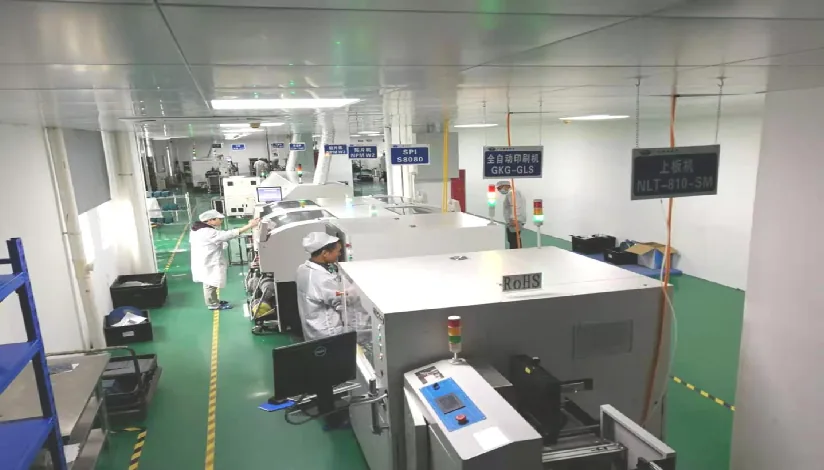
Wave soldering is a bulk soldering process for through-hole components. The board, with parts inserted from the top, travels on a conveyor over a pumped wave of molten solder. As the bottom side touches the wave, solder wets every exposed lead and pad, rises up the plated holes, and forms all the through-hole joints on that side in a single pass.
Before the wave, the board is sprayed with flux and preheated. After it, the joints cool and solidify. That sequence of flux, preheat, wave, and cooling is the whole wave soldering process. Each step has its own settings, and most wave solder defects trace back to one of them or to the board layout.
Wave soldering is fast and repeatable on boards with many through-hole joints. It is less suited to boards whose solder side is crowded with surface-mount parts. This guide explains how the process works, what the solder wave profile controls, when to choose wave over selective soldering or reflow, and the layout rules that help a board solder cleanly.
Key takeaways
- Wave soldering solders all bottom-side through-hole joints at once by passing the board over a standing wave of molten solder.
- The four steps are fluxing, preheat, wave contact, and cooling. Preheat drives off flux solvent and brings the board up to temperature so the barrel fills.
- Many machines use two waves: a turbulent wave to reach into holes and around parts, then a smooth laminar wave to remove excess solder and reduce bridging.
- Bottom-side SMT parts must be glued and designed for the wave, or masked with a pallet. Otherwise selective soldering is usually the better route.
- Board layout drives yield: component orientation to the travel direction, lead protrusion, hole-to-lead clearance, and heat flow into planes.
What is wave soldering?
Wave soldering is a machine process in which the underside of a printed circuit board passes over a wave of molten solder to solder through-hole leads, and sometimes glued surface-mount parts, in one pass. The wave is created by a pump in the solder pot that pushes solder up through a nozzle, forming a continuously refreshed crest.
It was the main way to solder circuit boards before surface-mount technology. Today most boards are SMT and soldered by reflow, and wave soldering is used for the through-hole connectors, terminals, transformers, relays, and other large parts that remain. On a mixed-technology board, SMT reflow usually comes first (see the reflow soldering process), then through-hole parts are inserted and wave soldered.
APT's SMT and THT assembly line plans the build sequence, stencil, reflow, wave or selective soldering, and hand-add exceptions before release, so the through-hole step is decided rather than improvised.
When does wave soldering beat selective soldering for through-hole work?
| Step | What happens | What it controls | Typical problem if it drifts |
|---|---|---|---|
| 1. Fluxing | Liquid flux is sprayed or foamed onto the bottom of the board | Oxide removal on pads and leads; wetting | Too little: skips, poor hole fill. Too much: residue, solder balls |
| 2. Preheat | Bottom and often top heaters raise board temperature | Evaporates flux solvent, activates flux, reduces thermal shock, helps barrel fill | Too low: spatter, voids, poor fill. Too high: flux burned off before the wave |
| 3. Wave contact | Board passes over one or two solder waves at a set angle and speed | Contact time, wetting, hole fill, removal of excess solder | Short contact: insufficient fill. Long contact: heat damage, copper dissolution |
| 4. Cooling | Board leaves the wave and cools | Joint solidification, board stress | Movement while cooling: disturbed joints |
Step 1: Fluxing
Spray fluxers apply a controlled film of liquid flux across the bottom of the board. Foam fluxers pass the board over a foam head. The flux must reach every pad and wet the inside of the holes. The flux type also sets whether the assembly needs cleaning afterwards; the guide to solder flux types explains no-clean and water-soluble choices.
Step 2: Preheat
Preheat does three jobs. It evaporates the solvent in the flux so it does not boil and spatter in the wave. It raises the flux to the temperature where it becomes active. And it brings the board and component leads closer to solder temperature, so solder can climb the barrel before it freezes. Heavy boards and boards with large copper planes need more preheat than thin, sparse ones.
Step 3: Solder wave contact
The board crosses the wave at a slight upward angle. Dual-wave machines use a turbulent first wave that pushes solder into holes and around component bodies, then a laminar second wave that leaves cleaner joints and drains excess solder. The time each joint spends in contact with the solder is set by conveyor speed, wave height, and board angle.
Some machines run the solder pot under a nitrogen blanket to reduce oxidation and dross, which helps wetting on difficult finishes.
Step 4: Cooling
As the board leaves the wave, the joints solidify. Vibration or movement at this point can leave disturbed, grainy joints. After cooling, the board is inspected and, if the flux requires it, cleaned.
Wave pot temperature, dwell time, and contact length: which combination matches your lead pitch?
A solder wave profile is the temperature record of the board as it moves through the machine. Like a reflow profile, it is measured with thermocouples on the actual board, not inferred from machine setpoints. The elements to define are:
- Flux type and amount applied
- Preheat setpoints and the resulting board temperature at the wave, measured on the top and bottom
- Solder alloy and pot temperature
- Conveyor speed and angle, which together set contact time
- Wave height and whether one or two waves are used
- Atmosphere (air or nitrogen)
The exact values come from the flux and solder alloy datasheets, the component temperature ratings, and the board's thermal mass. Lead-free alloys generally need a hotter pot and are more aggressive toward copper than tin-lead, so contact time and the condition of plated holes need more attention. Record the profile as part of the first-article package so the same settings are used for later lots.
Wave vs selective vs pin-in-paste vs hand: which method for which through-hole part?
This is the decision table for through-hole parts on a given board. Read across the row that matches your situation.
| Board situation | Wave soldering | Selective soldering | Pin-in-paste (reflow) | Hand soldering |
|---|---|---|---|---|
| Many THT joints, bottom side clear of SMT | Best fit: all joints in one pass | Works, but slower per board | Possible only if parts survive reflow | Too slow and variable |
| Many THT joints, bottom side has some SMT | Possible with a pallet masking the SMT, or with glued wave-compatible SMT | Often the better fit | Possible for suitable parts | Too slow |
| Few THT joints on a dense mixed board | Pallet cost hard to justify | Best fit | Good if parts tolerate reflow | Acceptable for very low volume |
| THT parts that cannot take full wave heat | Risky | Better: heat is local | Usually not suitable | Acceptable with control |
| High thermal mass joints (heavy copper, large pins) | Good if preheat is sufficient | Good: dwell can be set per joint | Fill may be insufficient | Difficult to fill reliably |
| Prototypes and very small lots | Setup and tooling overhead | Programming overhead | Needs stencil changes | Often the practical choice |
| Rework and exceptions | Not used | Possible | Not used | Standard route |
Wave soldering wins on throughput when through-hole joints are numerous and the solder side is accessible. Selective soldering wins when SMT parts crowd the solder side or only a handful of pins need soldering. APT's selective soldering page puts it this way: wave favors broad exposure and suitable volume, selective favors defined through-hole locations with a workable nozzle path, manual soldering remains for exceptions and rework, and reflow primarily serves SMT, with pin-in-paste for some through-hole parts.
Most wave guides compare 2 methods. This table covers 4, including pin-in-paste and hand, with a part-by-part column you can use to route a mixed-technology board.
For more on the trade-offs between the three through-hole methods, see through-hole soldering basics.
Mixed-technology boards and pallets
On a board with SMT parts on the bottom side, a wave would wash over them. There are two ways to handle it. Small passive SMT parts can be glued to the bottom side and designed with pad shapes and orientation suited to the wave. Alternatively, the board rides in a pallet (a carrier, usually made of composite material) that covers the bottom SMT parts and opens windows only over the through-hole areas. The wave solder pallet and fixture guide covers pallet design rules and clearances.
Design rules for wave soldering
Layout decides most of a wave-soldered board's yield. These rules are general; the assembler's process review should confirm them for your specific machine and pallet.
- Orient connectors and multi-pin parts so their rows run in a consistent direction relative to board travel, and agree that direction with the assembler. Solder drains along the last pin in a row, which is where bridges form.
- Add solder thieving pads at the trailing end of fine-pitch through-hole rows where the assembler recommends them, to pull excess solder off the last pin.
- Keep lead protrusion below the board within the range your acceptance standard and the assembler expect. Very long leads drag solder and form icicles; very short leads may not show a proper fillet.
- Size the plated hole to the lead with enough clearance for solder to flow up the barrel, but not so much that it cannot fill.
- Use thermal relief connections where through-hole pins join large copper planes. A pin tied solidly to a plane sinks heat, and the barrel may not fill.
- Avoid placing tall bottom-side SMT parts directly ahead of through-hole pins in the travel direction. They shadow the wave and can cause skips.
- Keep bottom-side SMT parts that will see the wave to packages and orientations the assembler approves, glued in place.
- Leave conveyor edge clearance and tooling holes as the assembler requires, or plan a panel rail.
Common wave defects: bridges, icicles, blowholes, and the flux condition that drives each
| Defect | What it looks like | Common causes |
|---|---|---|
| Bridging | Solder joining adjacent pins | Pin orientation to the wave, no thieving pad, insufficient flux, contact time, lead protrusion |
| Insufficient hole fill | Solder does not rise fully up the barrel | Low preheat, heat sinking into planes, poor flux coverage, short contact, tight hole-to-lead clearance |
| Skips (open joints) | A pad with no solder | Shadowing by parts, flux not reaching the pad, gas trapped |
| Icicles | Spikes of solder hanging from leads | Long leads, low solder temperature, contaminated solder |
| Solder balls | Small spheres on the board or mask | Wet flux entering the wave, mask finish, excess flux |
| Blowholes and pinholes | Small voids in the fillet | Moisture or gas escaping from the hole wall, plating defects |
| Lifted components | Part lifted off the top surface | Wave pressure, unsupported parts, leads not clinched or held |
Before adjusting the machine, check where defects cluster. Bridges always on the same connector point to orientation or thieving. Poor fill only on ground pins points to thermal relief. Random skips point to flux coverage or shadowing.
Most guides list defects. This one lists the flux condition that produces each defect, so the fix is a process change, not a rework.
What to send for a wave soldering RFQ
- ODB++ or Gerber data, BOM, placement file, and assembly drawing showing which parts are through-hole
- Board thickness, copper weights, and which pins connect to large planes
- Bottom-side SMT layout, so the assembler can decide between glue, pallet, or selective soldering
- Connector specifications, lead finish, and lead length
- Solder alloy and flux restrictions, and whether cleaning or conformal coating follows
- Acceptance class (IPC-A-610 Class 2 or Class 3) and any hole-fill requirement beyond the standard
- Quantity and expected volume, which affect whether pallet tooling is worthwhile
APT's selective soldering page asks for the same core inputs for through-hole work: connector specifications, pin finish and protrusion, board thickness and copper information, alloy and flux restrictions, cleaning and coating requirements, and the required inspection and test evidence.
Why work with APTPCB on through-hole soldering?
APT decides between wave, selective soldering, pin-in-paste, and hand soldering during the engineering review, based on the board layout, part list, and volume. The THT step is released with controlled insertion, flux, preheat, solder temperature, dwell time, and post-solder inspection, and the solder profile is kept with the traveler alongside SPI, AOI, and test records.
Relevant standards and references may include:
- IPC J-STD-001: requirements for soldered electrical and electronic assemblies
- IPC-A-610: acceptability of electronic assemblies, including through-hole fill
- IPC-7530: guidelines for temperature profiling for mass soldering processes
- IPC J-STD-004: requirements for soldering fluxes
Frequently asked questions
What is wave soldering used for?
Wave soldering is used to solder through-hole components such as connectors, terminals, transformers, and relays in a single pass. It can also solder small surface-mount parts glued to the bottom side when the board is designed for it.
What are the steps of the wave soldering process?
The wave soldering process has four steps: flux is applied to the bottom of the board, the board is preheated, the bottom side passes over one or two waves of molten solder, and the joints cool and solidify. Inspection and, where needed, cleaning follow.
What is the difference between wave soldering and reflow soldering?
Wave soldering applies molten solder from a wave to the bottom of the board and is used mainly for through-hole parts. Reflow soldering melts solder paste printed on pads before placement and is used for surface-mount parts. Mixed boards often use reflow first, then wave or selective soldering.
When should selective soldering be used instead of wave soldering?
Use selective soldering when the solder side has surface-mount parts that a pallet cannot protect, when only a few through-hole joints need soldering, or when some joints need their own heat and dwell. Wave is faster when many through-hole joints are accessible on the bottom side.
What causes bridging in wave soldering?
Bridging usually comes from pin orientation relative to the wave direction, a missing solder thieving pad at the end of a row, insufficient or uneven flux, too-long leads, or contact settings. The pattern of where bridges appear on the board points to the cause.
Can SMT components go through wave soldering?
Some can. Small passive parts glued to the bottom side, with pads and orientation designed for the wave, are wave soldered on many boards. Fine-pitch ICs, BGAs, and bottom-terminated parts should not see the wave; they are reflowed and masked with a pallet, or the board uses selective soldering instead.
Wave soldering quote checklist
Use this when you request a wave soldering or mixed-technology assembly quote.
- Mix of THT and SMT on the same board: state approximate THT/SMT ratio
- Single-sided or double-sided wave: state which
- Process: wave soldering, selective soldering, or pin-in-paste (state which per area)
- Pallet or fixture required Y/N, and who supplies it
- Wave temperature: 250 ±5 °C target or state your profile
- Preheat zones: 3, 4, or 5 zones (state which)
- Flux type: no-clean, rosin, or water-soluble (state which)
- Compatible through-hole diameter range: 0.8–1.5 mm (confirm all THT parts fit)
- Bridging risk assessment required Y/N; state any high-risk component orientations
- Target bridging and leads defect rate or DPMO baseline
- IPC-A-610 acceptance class: Class 1, 2, or 3
- Rework permitted and which method: hand solder or selective
- Line 0 nitrogen atmosphere required Y/N
Choose the through-hole route early
Wave soldering is efficient when the board is designed for it: through-hole joints accessible on one side, consistent pin orientation, thermal relief on plane pins, and a clear plan for any bottom-side SMT. Make that decision during layout, not after the first build, and let the assembler confirm which of wave, selective, pin-in-paste, or hand soldering each part will use.