
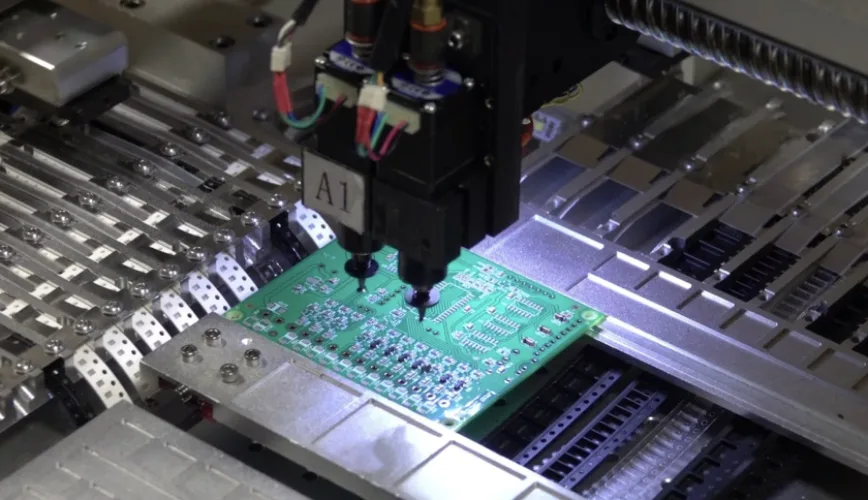
Reflow soldering is the method used to solder surface-mount components to a printed circuit board. Solder paste, a mix of tiny solder alloy particles and flux, is printed onto the pads. Components are placed into the wet paste. The board then travels through a reflow oven that heats it along a controlled temperature curve, melts the paste so the solder wets the pads and leads, and cools it so the joints solidify.
"Reflow" means the solder is melted, or flowed, in place rather than applied as molten metal from outside. That is what separates it from wave soldering, where the board passes over a bath of liquid solder.
The oven gets most of the attention, but a reflow joint is decided at several points before the board ever enters it. This guide walks through the reflow soldering process step by step, explains what each oven zone controls, lists the common defects and where they start, and ends with the process records worth asking an assembler for.
Key takeaways
- The reflow soldering process has four production steps: paste printing, inspection, placement, and the oven. Each one can create a defect that the oven cannot fix.
- Inside the oven, the profile moves through preheat, soak, reflow (peak), and cooling. The paste maker's datasheet and the board's thermal mass set the limits, not a generic curve.
- Most reflow defects start upstream: stencil design, paste volume, placement offset, or component moisture.
- Nitrogen reflow lowers oxidation during the liquid phase. It helps fine-pitch and bottom-terminated parts, but it does not replace a correct profile.
- Ask for evidence tied to your board: the measured profile, SPI and AOI results, X-ray for hidden joints, and first-article records.
What is reflow soldering?
Reflow soldering joins surface-mount devices to a PCB by melting pre-applied solder paste in a controlled heating cycle. The paste does three jobs. Its flux cleans oxides from the pad and lead, its solder alloy forms the joint, and its tackiness holds parts in place until the solder melts.
As the paste melts, surface tension pulls the molten solder onto the wettable metal and can draw slightly offset parts back toward the pad center. When the board cools below the alloy's melting point, the solder freezes into a fillet. A good joint has formed an intermetallic bond with both the pad and the component termination.
SMT soldering today is almost entirely reflow. (For the wider surface-mount process and terminology, see what SMT is and how it works.) It handles chip resistors and capacitors, gull-wing ICs, QFNs, BGAs, and many connectors in one pass. Through-hole parts are a different case, covered further down.
Reflow soldering process step by step
A reflow line usually runs in this order:
- Solder paste printing. A stainless steel stencil is aligned over the board and a squeegee pushes paste through its apertures onto the pads. The stencil thickness and aperture size set how much solder each joint gets.
- Solder paste inspection (SPI). A 3D SPI system measures paste height, area, and volume on every pad and flags bridging, missing paste, and offsets before any part is placed.
- Component placement. Pick-and-place machines take parts from feeders and set them into the paste at programmed coordinates, using the board fiducials for alignment.
- Reflow. The board passes through the oven on a conveyor. The temperature profile melts the paste and forms the joints.
- Post-reflow inspection. AOI checks visible joints, polarity, and placement. X-ray (AXI) checks joints hidden under BGAs, QFNs, and other bottom-terminated parts.
Double-sided boards repeat the cycle. The side with lighter parts is usually reflowed first, then the board is flipped and the second side is printed, placed, and reflowed. Parts on the first side go through the oven twice, so heavy parts on that side may need adhesive or a design review.
APT's SMT and THT assembly page lists 3D SPI before reflow, AOI after SMT and THT soldering, and targeted AXI for hidden joints as the typical release path.
Reflow oven zones explained
A convection reflow oven is divided into heated zones along the conveyor, followed by cooling zones. Each zone is set to a temperature, and conveyor speed decides how long the board spends in each. Together they produce the board's thermal profile. More zones give finer control over the shape of the curve. APT's assembly lines list 10-zone nitrogen reflow ovens.
The profile itself is usually described in four stages:
| Stage | What happens | What it controls | If it goes wrong |
|---|---|---|---|
| Preheat | The board warms from room temperature at a controlled ramp rate | Solvent evaporation, thermal shock to ceramic parts | Too fast: solder balls, spatter, cracked capacitors. Too slow: flux used up early |
| Soak (thermal equalization) | Temperature rises slowly or holds below melting | Brings large and small parts closer in temperature; activates flux | Too short: uneven melting, tombstones. Too long: flux exhausted, poor wetting, voids |
| Reflow (peak) | The board rises above the alloy's liquidus and peaks | Wetting and intermetallic formation | Too low or short: cold or grainy joints, head-in-pillow. Too high or long: component and laminate damage, excess intermetallic |
| Cooling | Temperature falls back below solidus | Grain structure of the joint, board stress | Too slow: coarse grain. Too fast: stress on large parts and the board |
The exact numbers for ramp rate, soak time, peak temperature, time above liquidus, and cooling rate come from the solder paste datasheet and the component ratings, then get tuned to the board's thermal mass. The guide to reflow profile basics: soak time, peak, and delta-T covers those parameters and how to read a profile graph.
Oven setpoints are not board temperatures
A zone set to a given temperature does not mean the board reaches it. Heavy copper planes, large connectors, and BGAs heat more slowly than small passives. The only way to know what the joints saw is to profile the actual board: attach thermocouples to the hottest and coldest locations, run it through the oven, and compare the curve to the paste's process window. The spread between the hottest and coldest point is the delta-T.
Thin boards and very heavy boards both need their own profile. APT has a separate note on reflow profiling for thin boards, where warpage becomes the main risk.
Process control points: what to check at each step
This is the table to use when reviewing an assembler's reflow process or debugging a yield problem. It maps each step to the parameters that matter, the defect it produces when it drifts, and the inspection gate that catches it.
| Process step | Control parameters | Defects when out of control | Where it is caught |
|---|---|---|---|
| Paste handling | Storage temperature, thaw time, open time, lot traceability | Poor print release, dry paste, solder balls | Print inspection, SPI trend |
| Stencil | Thickness, aperture size and shape, area ratio, step areas, cleaning interval | Insufficient or excess solder, bridging, voids under thermal pads | SPI volume and area |
| Printing | Alignment, squeegee pressure and speed, separation speed, board support | Offset paste, smearing, bridging | SPI on 100% of pads |
| Component handling | Moisture-sensitivity level, floor life, bake records | Popcorning, delamination inside packages, voids | X-ray, cross-section on failure |
| Placement | Placement accuracy, nozzle condition, part data (size, polarity) | Skew, wrong polarity, missing parts, tombstones | Pre-reflow AOI where used, post-reflow AOI |
| Reflow profile | Zone setpoints, conveyor speed, atmosphere, measured board profile | Cold joints, head-in-pillow, voids, tombstoning, overheating | Profile record, AOI, X-ray |
| Cooling and handling | Cooling rate, conveyor exit, board support | Disturbed joints, warpage | AOI, flatness check |
| Second side (double-sided) | Part weight on first side, second-pass profile | Parts falling off, re-melted joint defects | AOI, X-ray |
Defects caught at SPI are cheap to fix: wipe the board and reprint. Defects caught after reflow mean rework, and rework is a second thermal cycle on the board and its parts. That is why SPI is one of the most useful gates in the line.
For stencil rules on fine-pitch and small passives, see the stencil design rules for fine-pitch PCBA. For paste choice, see how to select solder paste.
Reflow vs wave soldering
Both methods make solder joints. They suit different parts.
| Reflow soldering | Wave soldering | |
|---|---|---|
| Solder source | Paste printed before placement | Molten solder bath under the board |
| Main parts | Surface-mount devices | Through-hole parts, some bottom-side SMT glued in place |
| Heat exposure | Whole assembly goes through the oven | Bottom side contacts the wave; top side is heated indirectly |
| Tooling | Stencil per board side | Pallets or fixtures if SMT parts sit on the solder side |
| Typical use | Almost every modern SMT board | Boards with many through-hole connectors and few bottom-side SMT parts |
Many boards need both. SMT parts are reflowed first, then through-hole parts go through wave, selective soldering, or hand soldering. Some through-hole parts can also be reflowed using pin-in-paste, where paste is printed into and around the hole. That works when the part can survive the reflow profile and the hole and lead geometry allow enough solder fill.
The wave soldering process guide covers the wave steps and design rules, and the selective soldering service page explains when localized through-hole soldering is a better fit than a full wave.
Nitrogen vs air reflow
Reflow can run in air or in a nitrogen atmosphere. Nitrogen displaces oxygen in the oven, so the molten solder and the metal surfaces oxidize less during the liquid phase. The practical effects are better wetting on difficult finishes, shinier joints, and a wider process window for fine-pitch and bottom-terminated parts.
Nitrogen adds running cost and is not needed on every board. It does not fix a bad stencil, a wrong profile, or damp components. Treat it as one more control, specified when the parts or finish call for it. APT's BGA and fine-pitch assembly process uses nitrogen reflow with thermocouple profiling and a published delta-T target of 5 °C or less across the board.
Common reflow soldering defects
| Defect | What it looks like | Usual starting point |
|---|---|---|
| Solder bridging | Solder joining two adjacent leads or pads | Excess paste, smeared print, misaligned stencil, poor pad design |
| Tombstoning | A small chip part stands up on one end | Uneven heating or paste volume between the two pads, placement offset |
| Solder balls / beading | Small spheres of solder near the joint or beside chip parts | Fast preheat, paste moisture, excess paste, aperture shape |
| Voids | Gas pockets inside the joint, visible on X-ray | Flux outgassing under large thermal pads, paste chemistry, via-in-pad, profile |
| Head-in-pillow | A BGA ball rests on the paste but does not merge with it | Warpage, oxidized balls, insufficient heat or flux activity |
| Cold or grainy joint | Dull, rough joint with poor wetting | Peak temperature or time above liquidus too low, contaminated surfaces |
| Non-wetting / dewetting | Solder does not spread or pulls back from the pad | Surface finish oxidation, contamination, exhausted flux |
| Component cracking | Cracks in ceramic capacitors or packages | Thermal shock, board flex after reflow, moisture in packages |
Before changing the oven, find out where the defect started. A tombstone on one footprint everywhere on the panel points to pad or stencil design. Tombstones scattered randomly point to placement or paste. Voids under QFN thermal pads respond to stencil window patterns as much as to profile, which the article on QFN reflow practices to reduce voids covers in detail.
Process records to ask for
When you qualify an assembler, or when a lot has a yield problem, these records show whether the reflow process is under control for your board:
- Measured reflow profile for your part number and revision, with the thermocouple locations and the paste's process window overlaid
- SPI data for the first article and the production lot, including any pads that were flagged and reprinted
- AOI results with defect categories and how false calls were resolved
- X-ray images and void measurements for BGAs, QFNs, and other hidden joints, against the acceptance threshold in your order
- Moisture-sensitive device handling records: floor life and any bake performed before placement
- First-article inspection report covering placement, polarity, and solder quality on the first board
- Change records if the stencil, paste, profile, or line changed between lots
Specify the workmanship standard in your order, usually IPC-A-610 Class 2 or Class 3, and state any void limits that differ from the assembler's default. APT keeps paste, reflow, THT solder, and electrical test logs tied to the traveler for each build.
What to send with an SMT assembly RFQ
- Gerber or ODB++ data including paste layers, plus the assembly drawing
- BOM with manufacturer part numbers and any approved alternates
- Placement (centroid) file with rotation and side
- Board finish and thickness, which affect wetting and thermal mass
- Solder alloy and flux requirements (for example lead-free, no-clean, or water-soluble) and whether cleaning is required
- Acceptance class, X-ray scope, and void criteria for hidden joints
- Quantity, build schedule, and whether a first article must be approved before production
Why work with APTPCB on SMT reflow assembly?
APT plans the build sequence, stencil, reflow, through-hole soldering, inspection, and test coverage before release, so mixed-technology boards do not reach the oven with an open question. The SMT reflow assembly line runs 3D SPI, AOI, and X-ray as standard gates, and first-article inspection with a measured profile locks the process for the production lot.
Relevant standards and references may include:
- IPC-A-610: acceptability of electronic assemblies
- IPC J-STD-001: requirements for soldered electrical and electronic assemblies
- IPC/JEDEC J-STD-020: moisture/reflow sensitivity classification for non-hermetic devices
- IPC/JEDEC J-STD-033: handling, packing, shipping, and use of moisture-sensitive devices
- IPC-7530: guidelines for temperature profiling for mass soldering processes
Frequently asked questions
What is the reflow process in soldering?
The reflow process prints solder paste on the PCB pads, places surface-mount components into the paste, then heats the assembly in an oven through preheat, soak, reflow, and cooling stages. The paste melts, wets the pads and leads, and solidifies into solder joints.
What are the four zones of a reflow profile?
The four zones are preheat, soak (thermal equalization), reflow or peak, and cooling. Preheat raises the board temperature at a controlled rate, soak evens out temperature and activates the flux, reflow takes the solder above its melting point, and cooling solidifies the joints.
What is the difference between reflow and wave soldering?
Reflow soldering melts paste that was printed on the pads before parts were placed, and it is used for surface-mount components. Wave soldering passes the bottom of the board over a wave of molten solder, and it is used mainly for through-hole parts.
Is nitrogen required for reflow soldering?
No. Many boards are reflowed in air. Nitrogen reduces oxidation while the solder is liquid, which helps wetting on fine-pitch parts, bottom-terminated packages, and some surface finishes. It is a process option, not a substitute for a correct profile.
What causes tombstoning in reflow soldering?
Tombstoning happens when one end of a small chip component wets and pulls before the other end melts. Common causes are unequal heating of the two pads, unequal paste volume, placement offset, and pad designs where one side connects to a large copper area.
Can through-hole components be reflow soldered?
Some can, using pin-in-paste. Paste is printed into and around the plated hole, the part is inserted, and the board is reflowed. The part must tolerate the reflow temperature, and the hole, lead, and paste volume must give enough fill. Otherwise wave, selective, or hand soldering is used.
Where a reflow joint is really decided
The oven melts the solder, but the joint is set by paste volume, placement, part condition, and a profile measured on the real board. When a reflow problem shows up, start at the gate that first saw it, usually SPI or AOI, and work back toward the step that caused it. When you choose an assembler, ask to see those records for a board like yours.