
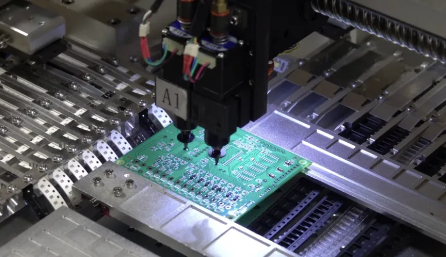
SMT, or surface mount technology, is the assembly method that solders components directly onto pads on the surface of a printed circuit board. No leads pass through holes. Solder paste is printed onto the pads, machines place the parts, and a reflow oven melts the paste to form the joints. Most electronics built today are assembled mainly with SMT because it allows small parts, dense layouts, components on both sides of the board, and fast automated placement.
The parts used in SMT are called SMDs (surface mount devices). SMT is the process, and an SMD is the component. This guide explains the difference, walks through how an SMT line works, compares SMT with through-hole technology (THT), and lists the surface mount PCB design rules that most affect assembly yield.
Key takeaways
- SMT means surface mount technology: the process of printing paste, placing parts, and reflowing them on the PCB surface.
- SMD means surface mount device: the resistor, capacitor, IC, or other part made for that process.
- A standard SMT line runs paste printing, solder paste inspection, placement, reflow, and automated optical inspection, with X-ray for hidden joints.
- SMT is the default for most parts. Through-hole remains the better choice for high mechanical stress, high current, and some connectors and large parts. Many boards mix both.
- Assembly yield is mostly decided in layout: land patterns, paste apertures, spacing, orientation, fiducials, and thermal balance.
SMT vs SMD: what is the difference?
People often write "SMD SMT" or "SMT SMD" as if they were the same thing. They are related but not interchangeable.
| Term | Full form | What it describes | Example usage |
|---|---|---|---|
| SMT | Surface mount technology | The assembly process and equipment | "The board is built on our SMT line." |
| SMD | Surface mount device | A component designed for surface mounting | "U3 is an SMD in a QFN package." |
| SMA | Surface mount assembly | A board assembled with SMT | Used in some older documents |
| THT | Through-hole technology | Leads inserted through plated holes | "J1 is a THT connector." |
An SMD has short leads, end terminations, or solder balls instead of long wire leads. Common SMD package families include chip resistors and capacitors (0201, 0402, 0603, 0805 and so on, named by size), SOT transistors, SOIC and QFP ICs with gull-wing leads, QFN and DFN packages with pads underneath, and BGAs with an array of solder balls.
How does an SMT line work?
An SMT production line is a sequence of machines connected by conveyors. A typical SMT process looks like this:
- Solder paste printing. A stainless steel stencil with apertures matching the pads is placed over the board, and a squeegee pushes solder paste through the openings. Paste volume is set by stencil thickness and aperture size. The SMT stencil design tutorial covers aperture rules.
- Solder paste inspection (SPI). A 3D inspection system measures paste height, area, and volume on every pad. Most solder defects start at printing, so this is the cheapest place to catch them. See solder paste inspection.
- Component placement. Pick-and-place machines take parts from reels, trays, or tubes, check them with cameras, and place them on the wet paste. The placement program comes from the centroid file and BOM.
- Reflow soldering. The board passes through a reflow oven with several heating zones: preheat, soak, reflow above the solder's melting point, and cooling. Paste turns into solid joints. The reflow profile basics explain how the profile is set.
- Automated optical inspection (AOI). Cameras check for missing, shifted, or wrong-polarity parts, bridges, and insufficient solder. The AOI basics guide explains what AOI can and cannot see.
- X-ray inspection. BGA, QFN, and other bottom-terminated parts have hidden joints, so X-ray is used to check voids, bridges, and missing connections under the package.
- Second side and through-hole. For double-sided boards, the process repeats on the other side. Through-hole parts are then soldered by selective soldering, wave soldering, or hand soldering.
- Test and final inspection. Flying probe, ICT, or functional testing, followed by final visual inspection and packing.
Two-sided SMT boards usually run the lighter side first, then flip and run the side with heavier or more heat-sensitive parts. Parts on the first side must stay in place during the second reflow, which is one reason heavy parts go on the top side.
SMT vs through-hole: which should you use?
Surface mount technology wins on density, cost per placement, and automation. Through-hole still wins where mechanical strength or current capacity matters. Most real boards are mixed technology: SMT for nearly everything, THT for a few connectors or power parts.
| Factor | SMT | Through-hole (THT) | Mixed technology |
|---|---|---|---|
| Component types | Passives, ICs, BGAs, QFNs, most modern parts | Large connectors, transformers, big electrolytics, relays, some power devices | SMT for most parts, THT for a few |
| Mechanical stress | Joints carry less load; can crack under repeated plug cycles or vibration if unsupported | Leads through the board resist pull and shear | Use THT or reinforced SMT for connectors that see force |
| Current and heat | Limited by pad size and copper; thermal vias help | Leads and barrels carry more current | Put high-current parts on THT where needed |
| Board density | High; both sides usable, no holes through inner layers | Lower; holes block routing on every layer | Moderate |
| Volume and cost | Lowest cost per joint at volume; fast automated placement | More manual or selective steps; slower | Extra process step for THT adds cost |
| Inspection | SPI, AOI, X-ray for hidden joints | Visual, AOI, barrel fill checks | Both sets of methods |
| Rework | Needs hot air or BGA rework stations | Easier with a soldering iron or desoldering tool | Plan rework for each type |
A simple rule: start with SMT for every part, then switch a part to through-hole only when you can name the reason, such as connector retention, current, heat, or a part that only exists in a through-hole package. The through-hole soldering basics explain how the THT step fits after reflow.
Most guides compare SMT vs THT as a binary choice. This table breaks the choice down by part type, so you can mix routes on one board without design rework.
SMT design rules that drive assembly yield, not placement convenience
Most SMT defects trace back to the layout. These rules have the largest effect on yield for a surface mount PCB:
- Use proven land patterns. Base footprints on the manufacturer's recommended land pattern or IPC-7351 guidance, and match them to the exact part number in the BOM.
- Keep pads symmetric on small passives. Unequal pad size or copper connection on the two ends of a 0402 or 0201 part causes uneven heating and tombstoning.
- Control thermal connections. Pads tied to large planes need thermal relief or extra preheat to reach reflow temperature with the rest of the board.
- Leave space between parts. Allow room for placement nozzles, AOI viewing angles, and rework. Keep tall parts away from fine-pitch parts that need inspection.
- Treat vias in pads deliberately. Open vias in pads can wick solder away from the joint. Either keep vias out of pads or specify filled and capped via-in-pad.
- Add fiducials. Place global fiducials on the board or panel and local fiducials near fine-pitch parts, with clear mask openings around them.
- Mark polarity and pin 1. Clear silkscreen marks reduce placement errors and speed up inspection. The SMT component polarity guide shows common marks.
- Plan the panel. Rails, tooling holes, and breakaway tabs must suit the conveyor and the depaneling method.
- Balance copper and think about warpage. Thin or unbalanced boards can bow in reflow and leave BGA joints open.
The design for assembly checklist collects these into a review list.
SMT defects and how they are caught
Even with good design, every SMT process has a defect spectrum. Knowing which inspection catches which defect helps you choose a test strategy.
| Defect | Typical cause | Best detection |
|---|---|---|
| Insufficient or excess paste | Stencil design, worn or clogged apertures | SPI |
| Solder bridge | Excess paste, misprint, tight pitch | SPI before reflow, AOI after |
| Tombstoning | Uneven pad heating or paste on small passives | AOI |
| Missing or shifted part | Placement, nozzle pickup, board movement | AOI |
| Wrong polarity or wrong part | Setup or feeder error | AOI, first-article inspection |
| Voids, hidden bridges, open BGA balls | Profile, paste, warpage, pad design | X-ray |
| Electrical faults | Wrong value, damaged part, open joint | Flying probe, ICT, functional test |
IPC-A-610 is the usual acceptance standard for soldered assemblies, with Class 1, 2, or 3 chosen by the product owner. The IPC-A-610 acceptance criteria overview explains how classes change the limits.
Most SMT guides list defects without the inspection method that catches them. This table pairs each defect with the best detection, so you can write the inspection plan from the defect list, not the other way around.
SMT assembly RFQ checklist
To quote SMT assembly accurately, a supplier needs to know what is on the board and how it should be built. Send a checklist that covers these items:
- Gerber or ODB++ data, including the paste layer for stencil design
- BOM with manufacturer part numbers, reference designators, quantities, and approved alternates
- Centroid (pick-and-place) file with X, Y, rotation, and side for each part
- Assembly drawing with polarity, special parts, and do-not-place items
- Lead-free or leaded process requirement, and any customer-specified solder paste
- Acceptance class (IPC-A-610 Class 2 or 3) and inspection requirements (X-ray on BGA, AOI, SPI)
- Through-hole parts and the preferred soldering method (wave, selective, pin-in-paste, hand)
- Test requirements: flying probe, ICT, functional test, programming
- Quantity per build, annual volume, and whether parts are turnkey, consigned, or hybrid
- Component packaging format (reel, tube, tray) and any dry-pack MSL handling
- Stencil thickness and aperture type (step-up, nano-coating, framed or frameless)
- Rework budget (number of touch-up cycles and what happens on X-ray reject)
- Conformal coating, potting, or underfill requirements
- Barcode or serialization requirement for traceability
The centroid file basics explain what the placement file must contain.
Why build your SMT boards with APTPCB?
APTPCB's SMT assembly services run on seven high-speed lines with a component window from 01005 chips up to 100 × 90 mm parts, ±25 µm placement accuracy, 10-zone nitrogen reflow, and 100% 3D SPI and AOI, with risk-based 3D X-ray. Through-hole parts are handled on the same order by dual-nozzle nitrogen selective soldering, which supports both lead-free and SnPb alloys, or by wave soldering. Acceptance follows IPC-A-610 and J-STD-001 at the class your drawing specifies.
Engineering review checks footprints, paste layers, panel design, and test access before the first build, so changes happen in the files rather than on the line.
Relevant standards and references may include:
- IPC-7351: land pattern requirements for surface mount design
- J-STD-001: requirements for soldered electrical and electronic assemblies
- IPC-A-610: acceptability of electronic assemblies
- J-STD-020 and J-STD-033: moisture sensitivity classification and handling of SMDs
Frequently asked questions
What does SMT stand for?
SMT stands for surface mount technology. It is the method of assembling electronic circuits by soldering components onto pads on the surface of a printed circuit board, rather than inserting leads through holes.
What is the difference between SMT and SMD?
SMT is the process of surface mounting. An SMD (surface mount device) is a component built for that process, such as a chip resistor, QFN, or BGA. You place SMDs using SMT.
What are the steps of the SMT process?
The main steps are solder paste printing, solder paste inspection, component placement, reflow soldering, and automated optical inspection. Boards with hidden joints also get X-ray inspection, and mixed-technology boards add a through-hole soldering step before test.
Is SMT better than through-hole?
SMT is better for density, automation, and cost at volume, and it is the default for most parts. Through-hole is better for parts that take mechanical force, carry high current, or only exist in through-hole packages. Many boards use both.
What is an SMT line?
An SMT line is the set of connected machines that assemble surface mount boards: a paste printer, SPI system, one or more pick-and-place machines, a reflow oven, and AOI, often followed by X-ray and test stations.
What files are needed for SMT assembly?
An assembler needs the Gerber or ODB++ data with a paste layer, a BOM with manufacturer part numbers, a centroid file, and an assembly drawing. Add test and programming requirements if the supplier will perform them.
Start from SMT, justify every exception
Surface mount technology is the default way to build a PCB assembly. Design every part for SMT unless there is a clear mechanical, electrical, or availability reason to use through-hole, follow land pattern and paste rules in layout, and give the assembler a complete data package. That combination gives the highest first-pass yield on a new board.