
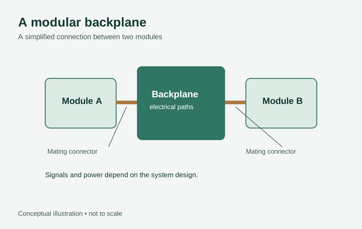
A backplane is a circuit board that connects plug-in cards or modules through mating connectors. It provides electrical paths between those modules and, in some systems, distributes power to them. Its other job is mechanical: the connectors must align with the cards and enclosure closely enough for reliable mating without excessive stress.
A backplane is not necessarily a shared bus, a high-speed board, or a power-distribution board. It can use shared signals, point-to-point links, or a combination. The terms passive, active, and midplane describe useful architectural distinctions, but none establishes a particular speed, topology, or power configuration.
How cards and connectors work together
A typical system has a backplane fixed inside a chassis. Individual cards slide into guides and mate with connectors on that board. The backplane traces then connect assigned contacts to other slots, a controller, a power input, or an external interface.
Depending on the architecture, those contacts may carry:
- Control, status, clock, or low-speed communication signals.
- High-speed point-to-point links between specified ports.
- Signals shared among several cards.
- Power and associated return currents.
- Identification or presence-detection signals.
Not every slot needs the same assignments. One slot might hold a controller while the others accept interchangeable I/O cards. The connector keying and pin assignments must prevent—or at least clearly address—the consequences of inserting the wrong card into a slot.
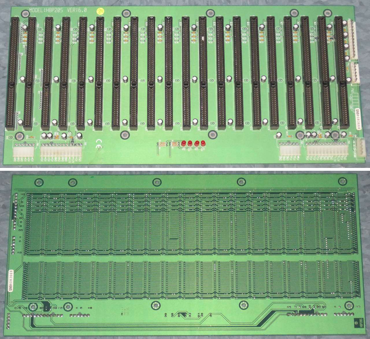
The photo illustrates a physical backplane, not a template for every system. Connector type, card orientation, signal routing, and power arrangements vary with the equipment.
Passive, active, and midplane: what the names mean
A passive backplane primarily interconnects its ports without actively processing the signals on those paths. It can still contain passive components, such as resistors or capacitors, if the design calls for them. Passive does not mean slow: a passive board can carry high-speed point-to-point links, provided the complete channel meets its requirements.
An active backplane includes active circuitry that participates in a function such as switching, buffering, signal conditioning, control, or power management. Adding active devices changes the design boundary: components need power, thermal provisions, assembly controls, and a way to test their operation. The word active alone does not say which of those functions are present.
A midplane generally sits between modules that connect from opposite sides. This packaging choice can help organize a system with accessible modules on both sides, but it also makes connector placement, clearance, assembly access, and airflow more involved. A midplane can be passive or active.
These descriptions are not specifications. Intel’s Server System SR2500AL Technical Product Specification, revision 1.6, describes passive SATA/SAS and active SAS/RAID mid-plane options for one server system. That is an example of how one product uses the terms, not a rule for other backplanes.
For an RFQ or design review, replace the label with the actual slot map, connections, components, and operating requirements.
Start with the mechanical fit
A backplane can pass an electrical test and still fail in the chassis. Before routing, define how each card reaches its connector and what supports it before, during, and after mating.
The mechanical handoff should identify:
- Mating parts: connector manufacturer, part numbers, revisions, keying, orientation, and the corresponding card-side parts.
- Reference geometry: board outline, datum scheme, mounting holes, slot pitch, connector location and orientation, card-guide positions, and enclosure interfaces.
- Board and connector fit: board thickness range, connector mounting method, hole or pad requirements, and applicable connector drawings.
- Clearance: component height, connector shrouds, fasteners, extraction hardware, neighboring cards, and access for assembly and service.
- Loads: expected insertion and extraction forces, support points, retention, and limits on board flex.
Use the connector manufacturer’s current drawings for the actual selected parts. For a press-fit connector, finished-hole requirements matter: nominal drill size alone is not an acceptance criterion. The connector supplier’s requirements and the PCB fabrication tolerances must be reconciled, including plating effects and the finished-hole range.
Treat alignment as a tolerance stack, not as a set of nominal coordinates. Board position, mounting-hole tolerance, connector placement, card-guide position, card thickness, and chassis variation can all contribute to mating error. A three-dimensional assembly model and a fit check with representative parts can expose interference or excessive misalignment before production.
If a fit check fails, do not immediately enlarge holes or shift a footprint. Identify which datum or tolerance contributed to the mismatch, check the mating-part revisions, and agree on a controlled drawing change. A local mechanical fix can alter connector reliability or card alignment elsewhere.
Define the topology before choosing routing rules
The schematic and slot map should say which ports communicate and whether each connection is shared or point-to-point. For each important path, identify the source, destination, connector transitions, card-side routing, and any required components.
A shared bus can have stubs and loading from multiple cards. A point-to-point link has a different set of concerns, but it still includes more than the trace on the backplane: card traces, connector contacts, vias, launches, and terminations all contribute to the channel.
For demanding links, agree on a channel budget that includes the relevant limits for loss, reflections, crosstalk, timing, and other requirements imposed by the interface. Then decide who owns each portion of the budget. A short backplane trace cannot compensate automatically for an unsuitable connector or a long card-side route.
Practical review questions include:
- Are connector pin assignments compatible with the required signal and return paths?
- Do differential pairs have a continuous reference path, including through layer transitions?
- Are via stubs, connector breakouts, unused branches, and adjacent channels accounted for?
- Where are termination and any required coupling components located?
- Which operating modes and slot populations create the worst channel conditions?
- Is the planned analysis based on the actual connector and board construction data?
Routing length is important, but “make every trace short” is not a complete design rule. Length matching, allowable skew, loss, and topology depend on the interface and its specified limits. If analysis shows insufficient margin, options might include changing the connector pinout, shortening or reassigning a route, revising the stackup, or changing the architecture. Adding an active device is another architectural choice, not a universal cure.
Amphenol’s Backplane vs. Cabled Backplane System discusses PCB and cabled approaches to interconnection. For either approach, qualify the particular connector and channel in the intended system rather than assuming a product category guarantees performance.
Power, return paths, and heat are separate decisions
Some backplanes distribute power; others do not. When power is present, the design needs an explicit map of inputs, outputs, returns, protection, and permissible slot loads.
For each rail, document the voltage range, current demand, startup or transient conditions, and which cards consume or supply it. Check connector contact ratings under the actual operating conditions. Ratings may depend on temperature, neighboring loaded contacts, airflow, and the connector manufacturer’s stated derating rules. Do not assume that adding contacts in parallel automatically produces an equal current split.
Power-integrity work also includes the distribution path: copper geometry, return paths, decoupling allocation, voltage drop, and the behavior of the source and loads. If the system must tolerate a card fault, hot insertion, or supply redundancy, define those requirements explicitly; they require more than a nominal current total.
Thermal review must consider heat from connector contacts, copper losses, components on an active backplane, and nearby cards. Card spacing and enclosure airflow affect the result. A midplane with modules on both sides can make airflow paths and access especially important to verify.
For a power-focused architecture, see redundant PSU backplane design. That discussion should not replace the current, protection, and fault analysis for the specific system.
Hypothetical example: a modular instrument
Invented example and assumptions: A proposed instrument has one controller card and four interchangeable measurement cards. All five cards plug into a mechanically supported backplane. The controller communicates with each measurement card over a separate point-to-point link. The backplane also distributes power from an external supply. No interface speed, connector family, stackup, current rating, or performance result is assumed here.
A useful design sequence would be:
- Allocate the slots. Define a controller slot and four measurement-card slots, including card-side orientation and keying. Decide whether the cards are truly interchangeable and what prevents an incompatible insertion.
- Map each link. Assign the controller-to-card connections and their return paths. Record the card-side and backplane-side portions of each channel rather than treating the backplane in isolation.
- Allocate power. Define the external supply connection, each card’s demand, return contacts, protection strategy, and required behavior during startup or a card fault.
- Check the enclosure. Model card guides, connector locations, mounting points, service access, and airflow. Evaluate the worst-case alignment across the stated tolerances.
- Set verification criteria. Agree on the electrical, mechanical, and thermal checks before ordering hardware. If a channel or fit check fails, revise the responsible interface and repeat the affected checks.
This example describes a possible architecture, not a measured instrument or an APTPCB product. A different instrument could use a shared bus, omit power distribution, or place active circuitry on the backplane.
Turn the design into a testable RFQ
A fabrication or assembly quote is more useful when the supplier can distinguish requirements from open decisions. The table below is a transfer checklist, not a claim that every project needs every test or that a particular service is available.
| Handoff item | Include when applicable | Condition or acceptance limit to define |
|---|---|---|
| Fabrication package | Revision-controlled manufacturing data, board outline, drill data, and netlist | Approved revision, finished dimensions, material and construction requirements, and disposition of conflicts |
| Connector interface | Exact mating parts, drawings, footprints, mounting method, and slot map | Finished-hole or pad requirements, placement tolerances, board thickness, and permitted mating alignment |
| Stackup and routing | Proposed layer arrangement, impedance-controlled nets, and critical paths | Target impedance, tolerance, reference layers, and approved substitutions; reconcile with the fabricator before release |
| Signal channels | Endpoints, topology, interface requirements, and connector data | Channel limits and analysis or measurement method, including the portions outside the backplane |
| Power and thermal | Rail map, current and transient assumptions, card population, and cooling conditions | Voltage-drop, temperature, contact-loading, and fault-behavior limits appropriate to the system |
| Assembly | BOM, approved alternatives, placement data, polarity, connector orientation, and assembly drawings | Process constraints, inspection criteria, and any restrictions from component suppliers |
| Verification | Bare-board electrical test needs, mechanical checks, and any assembly or system tests | Test scope, fixture or coupon requirements, sampling, pass/fail criteria, and responsibility for resolving failures |
The stackup should be a controlled agreement, not an isolated line in a layout tool. Board thickness and plating affect connector fit; dielectric and copper construction affect impedance and loss. If the proposed construction cannot meet a fabrication constraint, evaluate the effect on both mechanical fit and electrical performance before accepting a substitution. The PCB stackup design article provides additional context.
For an assembled backplane, separate three questions: does the bare board match the intended netlist, are the parts correctly installed, and does the complete system operate within its requirements? A bare-board continuity test does not establish signal-channel margin. Likewise, a coupon or fixture measurement is useful only if its structure, measurement method, and acceptance criteria are agreed in advance.
For a higher-speed example of channel-specific planning, see PCIe Gen 6 backplane PCB prototyping. The relevant limits must still come from the selected interface and system design.
Resolve exceptions before release
If information is missing, mark it as to be agreed rather than silently applying a generic value. Ask for a design review when connector hole requirements conflict with the proposed fabrication tolerances, when the impedance target conflicts with the thickness needed for mating, or when a critical channel has no budget for the card and connector portions.
For a failed prototype, preserve the board revision, test setup, slot population, and failure location. First distinguish a manufacturing or assembly discrepancy from an inadequate design assumption. Then correct the controlled documents and repeat the affected verification; a one-board rework is not, by itself, evidence that the released design is robust.
When the package is ready, submit the controlled files and open questions through APTPCB’s quote page. For unresolved interface or handoff questions, use contact before treating an assumption as an acceptance requirement.