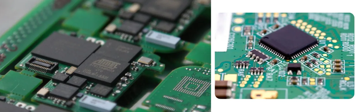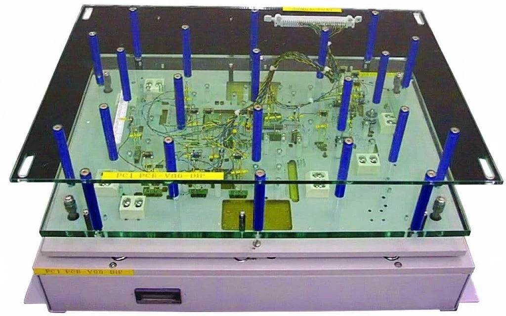
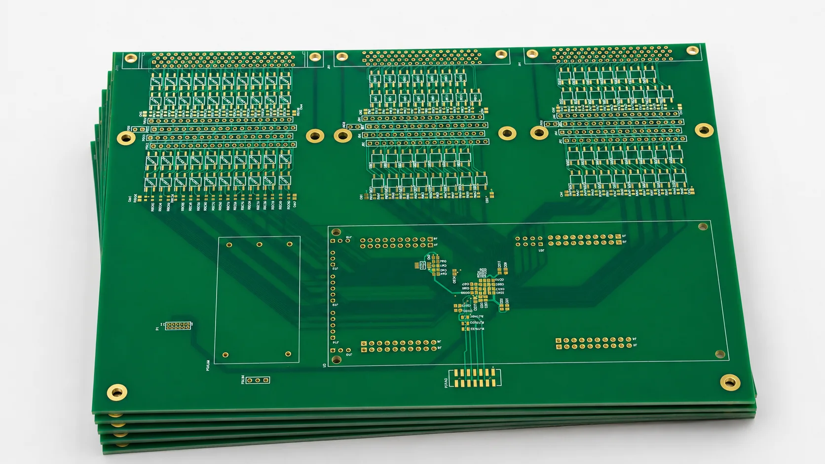
1. Ensure Accessibility to All Critical Nets:
- Strategic Placement – Distributing test points across the board to cover all necessary circuits
- Obstruction Avoidance – Designing layouts that prevent components or other board features from blocking probe access
- Dual-Side Coverage – Utilizing both top and bottom sides of the PCB for comprehensive test point placement