
Alumina and aluminum nitride (AlN) are ceramic substrate materials used when an electrical assembly needs insulation and a controlled path for heat. AlN grades can offer higher thermal conductivity; alumina may be sufficient when the complete thermal path meets the temperature target. Compare the exact grade, ceramic thickness, copper construction and cooling arrangement before choosing.
Start with the heat source, its contact area and the cooling arrangement. Then compare actual ceramic grades and substrate constructions. A more conductive ceramic can help when the ceramic is a significant part of the thermal path; it cannot compensate for every poorly conducting interface elsewhere in the assembly.
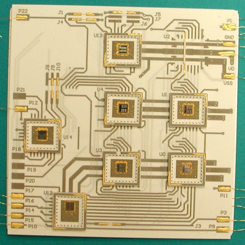
A multi-chip high-temperature ceramic circuit board. Source: NASA Glenn Research Center. The source does not identify the ceramic grade; this is not an APTPCB product.
First, identify which ceramic construction you need
A solid ceramic substrate has ceramic as the insulating body beneath the conductor. A ceramic-filled organic laminate is a different construction: ceramic particles are combined with a resin system, sometimes with glass reinforcement. Both may appear in electronics material searches, but their fabrication routes and properties should not be treated as interchangeable.
The ceramic itself is also a separate choice from its metallization. Direct bonded copper (DBC) and active metal brazing (AMB) describe ways of joining metal to ceramic. They are not alternative names for alumina and AlN. The available combination of ceramic, copper, geometry and bonding process needs to be confirmed for the project. Our DBC and AMB comparison examines the bonding decision in more detail.
Compare the complete thermal path
Heat from a semiconductor may pass through several layers before reaching a cold plate or surrounding air: die attach, copper, ceramic, another attachment layer and a cooling interface. Each contributes to the temperature rise. The heat also spreads as it moves, so the effective area at one layer is not necessarily the same as the die footprint.
Ask these questions before comparing conductivity values:
- How much heat must the device dissipate, and over what area does it enter the substrate?
- What is the allowable temperature at the component and at the cooling interface?
- What are the thickness and thermal properties of the proposed ceramic, copper and attachment layers?
- How will the substrate connect to the heat sink or cold plate, and what interface material is planned?
- Which assumptions need a thermal model, prototype measurement or both?
If a first-pass calculation suggests that the ceramic contributes relatively little to the total temperature rise, a more conductive grade may bring less system benefit than expected. If the ceramic dominates the path, AlN may merit a closer look. In either case, the comparison needs the actual grade, thickness and operating conditions. Our thermal interface material guide covers another part of that path.
Estimate the ceramic layer's contribution
For a first estimate of heat flowing through a uniform layer, the simplified relationship is R = t / (k × A), where R is thermal resistance, t is layer thickness, k is thermal conductivity and A is the assumed heat-flow area. The temperature drop across that layer is approximately heat flow multiplied by its thermal resistance.
For illustration, assume a 0.5 mm layer, a constant heat-flow area of 100 mm² and a heat flow of 20 W. Compare two hypothetical conductivities, 25 and 100 W/(m·K). These numbers are chosen to show how the calculation works; they are not properties of a specified alumina or AlN grade.
| Assumption | Conversion or result |
|---|---|
| Layer thickness | 0.5 mm = 0.0005 m |
| Heat-flow area | 100 mm² = 0.0001 m² |
| Hypothetical material, 25 W/(m·K) | 0.0005 / (25 × 0.0001) = 0.20 K/W; at 20 W, a 4°C drop |
| Hypothetical material, 100 W/(m·K) | 0.0005 / (100 × 0.0001) = 0.05 K/W; at 20 W, a 1°C drop |
Under these assumptions the ceramic-only difference is 3°C. Whether that matters depends on the device's remaining temperature margin and the rest of its thermal path. The estimate excludes die attach, copper, thermal interface and cooling resistance. It assumes steady, one-dimensional heat flow through a constant area and constant conductivity; real heat spreads and properties can change with temperature. It does not predict junction temperature. For a project comparison, replace the assumptions with data for the proposed grades and construction.
Reducing the ceramic thickness also reduces the resistance in this simplified equation. Thickness, however, is part of the insulation and mechanical design. Agree on an actual construction and its tolerances before treating a thinner substrate as an option.
Turn a temperature target into a comparison
Start with the maximum permitted device temperature under the relevant operating conditions and the expected temperature at the cooling boundary. The difference is the available temperature rise across the modeled path. Estimate the losses in the component and identify where they enter the assembly; then allocate the rise across the interfaces, substrate and cooling arrangement.
The cooling boundary itself needs a defined design. The PCB heat sink guide discusses the connection between a board, interface material and heat sink.
If the preliminary result is close to the limit, identify which inputs are least certain. Contact area, interface quality and cooling conditions may need measurements or sensitivity analysis. Compare candidate ceramics using the same assumptions first, then replace those assumptions with the proposed suppliers' grade-specific data. A lower calculated ceramic resistance should lead to a more detailed system check, not an automatic material release.
What else changes the material decision?
| Decision | What to compare | Question for the project team |
|---|---|---|
| Thermal performance | Conductivity of the proposed grade at relevant conditions, ceramic thickness and heat-flow area | Does the complete thermal path meet the device temperature target? |
| Electrical insulation | Substrate thickness, conductor layout, edges, environment and applicable test requirements | What voltage and insulation evidence does the assembled product require? |
| Mechanical behavior | Ceramic grade, copper pattern, mounting and expected handling or thermal cycling | Where could mechanical stress occur, and what evidence is needed? |
| Fabrication and assembly | Metallization, finish, geometry, attachment process and tolerances | Can the proposed construction and assembly process work together? |
| Supply and cost | Available grades, thicknesses, quantities and approved alternatives | What can be quoted, and what change would require a new approval? |
A bulk dielectric property is useful for comparing material data, but it is not automatically an insulation rating for an assembled module. Conductor spacing, edges, contamination, thickness and the relevant product requirements all matter. Likewise, a ceramic material should not be assumed to tolerate shock, vibration or repeated temperature changes without evaluating its actual construction and use.
Read a ceramic data sheet alongside the drawing
Two sheets may both say “alumina” while describing different grades, test specimens or temperatures. Record the manufacturer and exact grade, then check the stated conditions before transferring a property into a model. If conductivity is reported for a particular direction or temperature, preserve that detail; if the sheet does not state it, ask rather than filling in an assumed value.
For electrical insulation, note the reported property, specimen thickness and test method. For mechanical comparison, distinguish a material property measured on a defined specimen from the behavior of a substrate after copper bonding, cutting, assembly and mounting. A single conductivity, strength or dielectric figure cannot replace the proposed assembly drawing.
The comparison should also identify the copper construction and surface finish. A material grade may be suitable in principle while the requested conductor geometry, substrate size or finish still needs a separate manufacturing review. Send the drawing and the material specification together so the supplier can flag incomplete or incompatible requirements.
Consider handling and thermal cycling early
Ceramic substrates require attention to mechanical loads during fabrication, transport, assembly and service. Ask where the substrate is supported, how it is clamped to the cooling surface and whether a screw, connector or cable can apply a local load. Document the proposed attachment materials and the expected assembly temperatures.
Copper, ceramic and neighboring materials can respond differently to temperature changes. The resulting behavior depends on the complete construction, including copper pattern and thickness, ceramic grade, interfaces and thermal exposure. A material's expansion coefficient alone is not a lifetime calculation. If the application needs cycling evidence, define the assembly configuration, temperature or power profile, inspection method and acceptance criteria for the project.
Alumina and AlN should also be evaluated as finished, metallized substrates rather than judged solely by the bare ceramic. Ask for handling, cleaning, storage and assembly instructions that apply to the actual construction. A suitable procedure for one grade or metallization route should not be assumed to apply to every other one.
Where the design calls for solder attachment, review the proposed finish and thermal profile with the assembly team. The guide to soldering on ceramic discusses attachment considerations in more detail.
What would change the decision?
If the thermal model shows that the interface to the cold plate accounts for most of the temperature rise, improving that interface may be more useful than changing the ceramic. If the ceramic contribution is large, the team can compare a more conductive grade against the added cost and other design constraints. Either finding still needs to be checked against insulation, mounting and manufacturing requirements.
If only one material is available in the required thickness and copper construction, the practical decision may shift to a revised stack or a change in cooling. Record which requirement drives that change and obtain approval before replacing a specified grade. A substitute that looks similar on a thermal-property table may require different processing or new qualification evidence.
Information to include in an inquiry
Provide the intended material or alternatives, the ceramic thickness and tolerance, conductor pattern and copper requirements, and the required surface finish. Add the heat load and cooling interface, the operating voltage and environment, the mounting arrangement, and any expected assembly or service thermal cycles.
Identify which requirements are fixed and which can be discussed. Ask what material grades and construction options are available for the order, what data applies to each option, and how proposed substitutions will be approved. If you have an existing stack or material specification, include its revision and any relevant drawings.
For broader comparisons, start with the PCB material selection guide. To discuss a proposed construction, request a quote or contact APTPCB; confirm material and process availability during quotation.