
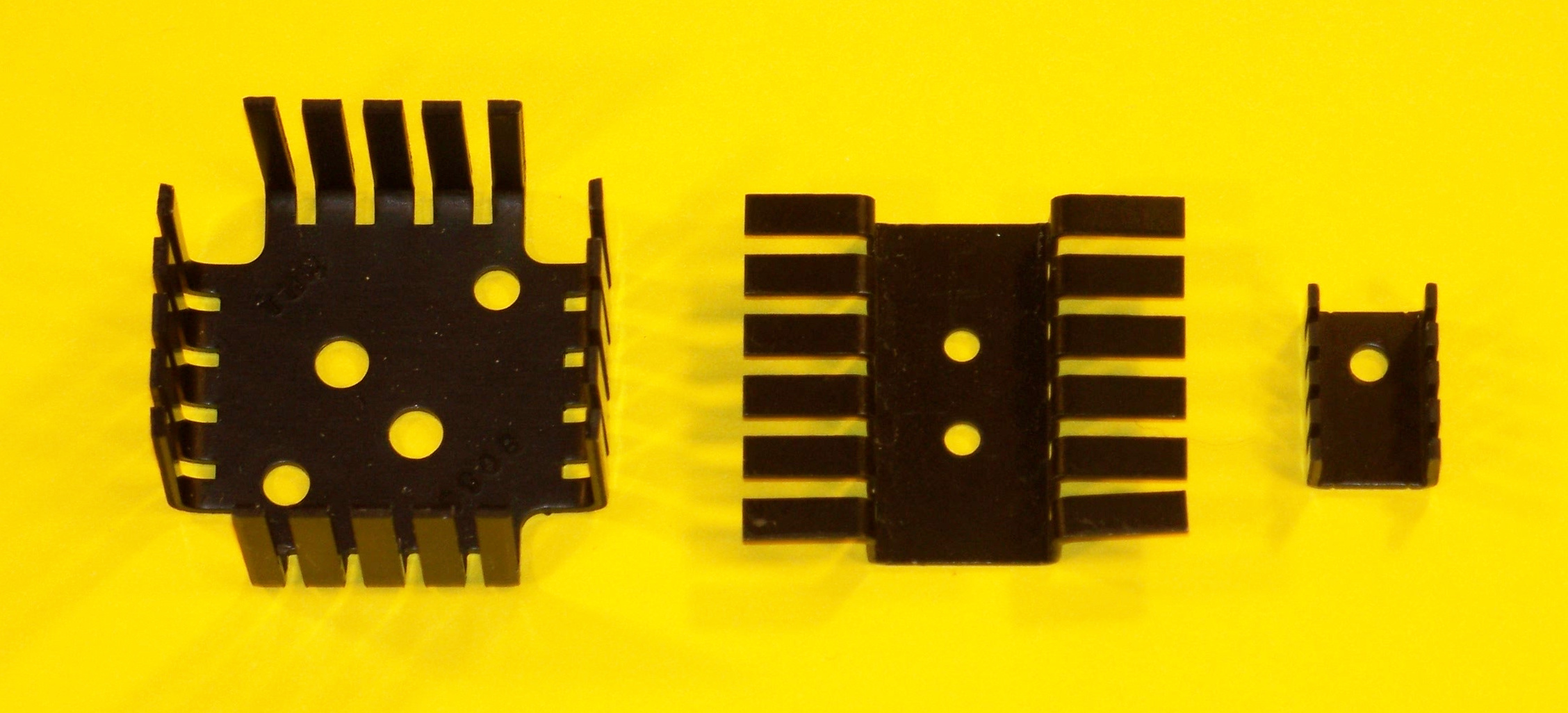
A PCB heat sink helps carry heat from a component to the surrounding air or a chassis. Its performance depends on the entire heat path. A sink that works in open air may perform differently inside an enclosure, while a device that sends most of its heat through its underside may benefit more from a board-to-chassis path than from a sink on top.
Trace heat from the device to the proposed sink and onward to its surroundings. Check that path under the actual mounting, airflow, enclosure and operating conditions.
Identify the paths out of the device
A component can lose heat through several routes at once. The PCB may be a major heat path, a supporting path, or a parallel path to a sink attached elsewhere. Do not assume that every watt travels through the same series of materials.
Three arrangements are useful starting points:
- Device-mounted sink: The sink contacts an appropriate surface of the package, generally through a thermal interface material (TIM). Heat crosses the package and interface into the sink, then leaves through the surrounding environment. Check whether the package surface is intended for this use and whether the package can tolerate the attachment method.
- Board-coupled sink: Heat travels from the device into PCB copper, potentially through thermal vias, and into a sink or other cooling surface coupled to the board. The copper, vias, board construction and contact area all influence the path.
- Chassis-mounted path: Heat reaches an enclosure or chassis through a package or board interface and mounting arrangement. The chassis must have a credible route for rejecting that heat to its surroundings; being mechanically large does not by itself establish sufficient cooling.
These approaches can coexist. For example, a top-mounted sink may remove some heat while the PCB carries the rest toward nearby mounting points. The division changes with construction and boundary conditions, so treating the routes as one fixed series chain can mislead a design decision.
Gather the inputs before selecting a sink
Start with the device and the conditions it will see in the assembly.
Heat source and loss. Identify each relevant heat-generating component and its dissipated power over the operating profile. Electrical input power is not automatically the heat generated by the component: account for power delivered elsewhere and other device-specific behavior. Record peak, sustained and duty-cycle conditions, including neighboring sources that can warm the same board or air.
Temperature limit and reference. Establish the permissible junction temperature or specified measurement-point limit from the applicable device documentation, including any margin required by the project. Record where temperature can actually be measured. A package-top measurement, a board measurement and ambient temperature are not interchangeable.
Package and thermal information. Determine where heat can enter or leave the package and which thermal metrics apply to the intended estimate. Package construction, exposed pads and the device manufacturer’s recommended board layout can determine whether a top-mounted or board-coupled approach is credible.
Ambient and enclosure. Define the worst credible ambient at the assembly’s operating location. Consider how enclosure heating, adjacent components and restricted openings affect the air reaching the sink. Ambient for a calculation or test should be defined consistently; room temperature outside a closed enclosure is not necessarily the air temperature around the device.
Space, airflow and orientation. Record the volume available for the sink, interface and mounting hardware. Include keepouts, assembly access and airflow paths. Orientation can affect natural convection, while fans, nearby obstructions and recirculation can change forced airflow. A sink’s published rating is tied to the manufacturer’s test conditions; those conditions may differ substantially from the installed assembly.
Installation and electrical constraints. Identify permissible attachment surfaces, electrical isolation needs, clearances and allowable mechanical loads. Decide whether the board or package needs support against mounting forces and handling. The best thermal contact is not useful if the installation creates an electrical fault or stresses the assembly.
Build a thermal budget without mixing metrics
A thermal budget connects heat loss to the temperature rise the design can tolerate. As a starting concept, subtract the relevant reference temperature from the allowable junction or measurement-point temperature. That gives the available temperature rise for the selected condition. The design must then provide a heat path that keeps the device within that allowance at the credible operating loss.
For an illustrative single series path, a temperature rise can be estimated by multiplying heat flow by the sum of the applicable thermal resistances. This approximation is useful only when the resistances describe the actual path, their boundary conditions match, and heat traveling through parallel routes has been accounted for. A path from package to sink to air is not automatically the whole system if the PCB also conducts substantial heat away.
Be especially careful with package datasheet metrics:
- Do not add a datasheet junction-to-ambient resistance, RθJA, to a separate sink-path resistance. RθJA reflects a defined test board and environment and can change strongly with board construction, airflow and surroundings. Adding a sink path to it as though it were a package-only resistance can double-count or misrepresent heat flow.
- Do not treat a psi metric as a thermal resistance. A thermal characterization parameter relates a junction temperature estimate to a specified reference measurement under its defined conditions; it is not interchangeable with a resistance for an arbitrary series network.
- Match each metric to its reference temperature and definition. A value intended for one measurement point or test condition should not be applied to another without the manufacturer’s guidance.
Texas Instruments, Semiconductor and IC Package Thermal Metrics, SPRA953D, explains the dependence of package metrics on their test conditions and the distinction between resistance and characterization parameters. Use the device manufacturer’s guidance for measurement and modeling. An estimate is a screening tool; it does not establish installed performance when the heat-flow split or boundary conditions are unknown.
Design the board-side path
Copper can spread heat away from a component and distribute it toward a sink, chassis contact or other area of the board. Its effectiveness depends on the available copper geometry, layer connections, nearby heat sources and where heat can leave the assembly. A large copper area trapped inside a warm enclosure may spread heat without rejecting enough of it.
Thermal vias can connect copper regions on different layers and help move heat away from an exposed pad or other device contact. Their contribution depends on the complete stackup and fabrication details. More vias do not guarantee a linear improvement: the limiting step may instead be the package interface, copper spreading, board-to-sink contact or heat rejection outside the board.
For board construction options, see APTPCB's high-thermal PCB selection page. Where vias enter a solderable pad, the via-in-pad manufacturing guide explains the related fabrication and assembly decisions.
Coordinate the layout with fabrication and assembly requirements:
- Identify which copper layers the vias connect and whether those connections are electrically permissible. A thermal pad or chassis contact may have a specified electrical potential or require isolation.
- Document via location relative to solderable pads. Vias in or near a pad can draw solder away during assembly, affecting the joint. Agree on an appropriate treatment with the parties responsible for fabrication and assembly rather than assuming every via is copper-filled or otherwise closed.
- Preserve the solderable area and connection details required by the device. Thermal changes must not compromise the electrical function or manufacturability of the pad.
- Check stackup, copper features and via details against the intended process before release. A drawing that says only “add thermal vias” leaves important choices unresolved.
- Consider how the board is supported at the sink or chassis contact. A thermal interface cannot compensate for excessive board flex, poor alignment or contact lost during installation.
NXP AN11753 gives via and heat-sink guidance for a specific device. Texas Instruments TIDA030 also illustrates a device-specific thermal path. Apply their guidance to the devices and conditions they cover, rather than treating their dimensions or performance as universal.
Make the interface and mounting work together
A sink needs repeatable contact with the surface it is intended to cool. TIM fills imperfections between mating surfaces, but its installed behavior depends on the selected material, contact area, bond line and mounting conditions. A drawing should define how the interface is applied or installed, not just name a material family.
Check flatness and tolerances across the package, board, sink and any chassis contact. Determine how mounting hardware establishes contact and whether it applies load where the package and board can safely carry it. Include mechanical retention, installation access and any support needed to prevent bending. Avoid relying on an assumed contact pressure or bond line that the assembly cannot consistently achieve.
Electrical isolation can add another interface to the path. Where isolation is required, evaluate the complete interface and mounting arrangement against both thermal and electrical requirements, including clearances and the hardware itself. An insulating layer is not a substitute for verifying the assembled design.
For a closer look at material selection, see thermal interface material selection. For LED-specific optical, mounting and thermal considerations, see PCB thermal management for LEDs.
Hypothetical comparison: top sink or board-to-chassis?
Hypothetical scenario: A designer is integrating a non-LED power device into an enclosed assembly. There is some space above the package, and part of the board is near a chassis mounting surface. Both a top-mounted sink and a board-to-chassis path appear mechanically possible. No cooling result is assumed.
A top-mounted sink is a candidate if the device documentation supports heat transfer through the package surface, the sink can be retained without damaging the package, and useful airflow can reach it. The designer should also check whether the enclosure leaves enough space around the fins and whether nearby components preheat or obstruct the air.
A board-to-chassis path is a candidate if the package can transfer heat effectively into the PCB, the stackup and copper can carry it toward the contact, and the chassis interface is practical. The designer must check board support, interface tolerances, electrical isolation and how the chassis rejects heat in the installed environment.
Neither option should be selected solely because it offers more visible metal. The package may favor one route, while enclosure conditions or assembly constraints favor the other. A combined approach may be worth evaluating if each path is mechanically and electrically compatible.
Evidence checklist for the decision:
- Device loss over the operating profile, allowable temperature and applicable package guidance.
- Intended heat-transfer surfaces and the definitions of the thermal metrics used.
- Board stackup, copper and via details for the chassis-coupled option.
- Sink, interface and mounting dimensions and tolerances for each candidate.
- Enclosure orientation, airflow and credible ambient conditions.
- A measurement or modeling plan that represents each installed configuration, including parallel heat paths.
- Agreed acceptance criteria and an owner for resolving any failure or discrepancy.
Validate the installed assembly
Plan validation around both transient and steady operating conditions. A short high-loss event can produce a temperature peak that a long-term average obscures. Conversely, a design that survives a brief test may still accumulate heat during sustained operation. Define the operating sequence and the condition used to judge whether temperatures have stabilized; do not assume either test substitutes for the other.
Place and document measurement points so that the resulting temperatures can be interpreted using the applicable device guidance. Record the heat source operating state, ambient reference, enclosure configuration, orientation, airflow and mounting condition with each result. Where the junction cannot be measured directly, use the manufacturer’s prescribed method and state the assumptions and uncertainty of the estimate.
See PCB thermal imaging for additional context on interpreting surface-temperature observations.
| Observed issue | System-level check | Evidence needed |
|---|---|---|
| Device temperature rises during sustained operation | Check enclosure air, airflow obstruction, sink contact and other heat sources—not just sink size | Operating loss, ambient and local temperature records, installed configuration and contact inspection |
| Brief operating event produces a temperature peak | Check the actual loss and duration, thermal mass and measurement response | Time-aligned operating profile and temperature measurements, with test-point locations |
| Board near the device is hot but the chassis contact is cooler | Check copper and via path, contact location, interface fit and board support | Stackup and layout, interface dimensions, assembled contact evidence and temperatures at defined points |
| Results vary between assemblies | Check TIM application, tolerances, mounting sequence and airflow consistency | Assembly records, interface and hardware specifications, test setup and measured variation |
Assign an owner to the validation plan before testing begins. That owner should ensure the conditions and acceptance criteria are agreed, results are reviewed against the device and project limits, and changes are controlled. Device, mechanical, PCB and assembly owners may need to resolve different parts of a failure. A fabrication or assembly process check alone does not prove that the finished product meets its thermal requirements.
Project handoff checklist
Document the intended heat path and its assumptions in the release package so the responsible owners can assess later changes. Include:
- Heat sources: component identification, dissipated loss, operating states and duty profile, with the source of each assumption.
- Device limits: permissible junction or measurement-point temperature, package heat-transfer guidance, thermal metric definitions and their reference temperatures.
- PCB path: stackup, copper geometry, pad and via details, electrical connections and any fabrication or assembly requirements affecting solder or contact.
- Sink and interface: dimensions, contact surfaces, TIM specification, intended bond line, mounting method, flatness and assembly tolerances.
- Electrical and mechanical constraints: isolation, clearances, hardware, board support, installation loads and access requirements.
- Environment: enclosure configuration, orientation, airflow, chassis contacts and credible ambient conditions.
- Validation: test points, operating sequence, transient and sustained conditions, acceptance criteria, measurement method and responsible owner.
- Change control: which sink, TIM, hardware, board, enclosure or airflow substitutions require review and revalidation, and who approves them.
When discussing the board with APTPCB, share the heat sources and power dissipation, stackup and via details, and sink and assembly interfaces. Contact APTPCB or request a quote, and include the validation requirements. Confirm the scope of any heat-sink assembly or thermal testing for your project.