
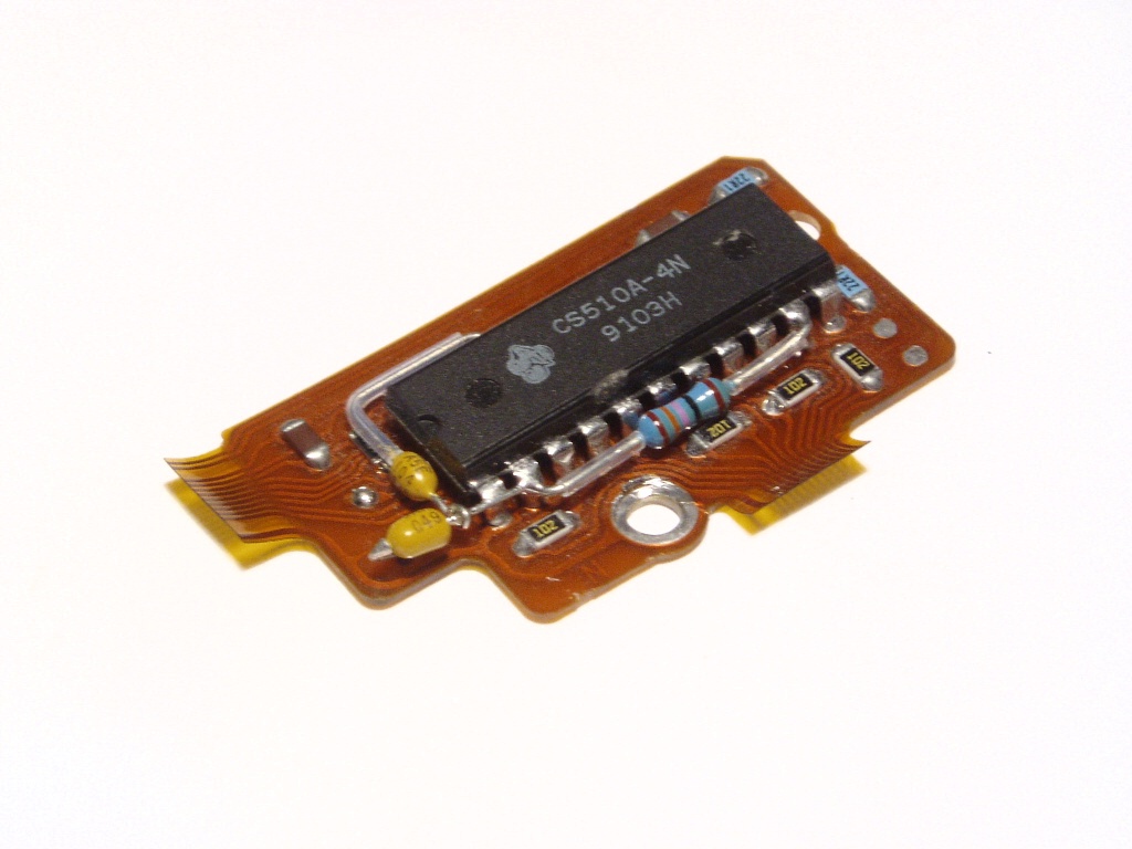
Choosing flex PCB materials means specifying the complete construction: the core film, copper, protective layers, adhesives and local reinforcement. The design must suit installation, any repeated movement, the electrical requirements and the way the circuit connects to the assembly.
Define the bend and operating conditions before selecting a candidate stackup. Ask the fabricator to confirm that it can produce the construction, then validate the finished circuit in its intended assembly. A material data sheet or a successful fabrication process alone does not establish finished-product qualification.
For a broader comparison with rigid substrate families, see the PCB material selection guide.
APTPCB's flex PCB manufacturing page provides a starting point for discussing the proposed construction.
What makes up a flex PCB material construction?
A flexible circuit may be thin, but it is not necessarily a single uniform sheet. Its layers have different jobs, and each can affect bending, electrical behavior or assembly.
- Core film: The insulating film supports the conductor pattern and contributes to the mechanical and electrical behavior of the stack.
- Copper foil: Copper forms conductors, reference planes and pads. Foil type, thickness, grain orientation and pattern all matter to the design.
- Laminate adhesive, where used: An adhesive-based copper-clad laminate uses adhesive to join copper to the dielectric film. The adhesive is part of the construction and should be included in thickness and environmental assessments.
- Coverlay: A protective film applied over selected circuit areas, usually with openings for pads and interfaces. It is commonly attached with a separate coverlay adhesive.
- Bondply: A bonding layer used where parts of a construction must be joined. Its placement and properties can affect the finished stack and its response to heat and bending.
- Stiffeners and local reinforcements: Added material at selected locations can support a connector interface or another area that needs local rigidity. These areas and their transitions require their own dimensional and mechanical review.
Not every design includes every layer in every location. A bend region, connector end and reinforced mounting area may have different local thicknesses. The stackup should show where each layer is present as well as its nominal sequence.
PI, LCP, flex and rigid-flex are different kinds of terms
Polyimide, often abbreviated PI, and liquid crystal polymer, or LCP, are material classes. Flex and rigid-flex describe board architectures. A flexible circuit can use a particular material construction; a rigid-flex board combines rigid and flexible regions whose interfaces also need to be designed.
Do not treat all products within either material class as interchangeable. Properties and available constructions depend on the specific film, laminate and grade. For example, Kapton is a DuPont brand associated with specific film products and grades; it is not a synonym for every polyimide film.
Product documents can help establish a starting point. Examples include DuPont Kapton HN data, UBE UPILEX information and Panasonic FELIOS material information. Qnity Electronics Pyralux AP is a particular adhesiveless, double-sided polyimide copper-clad laminate—not a description of every PI construction. Review the documents for the actual candidate product and ask the fabricator to confirm its proposed construction before relying on a property in the design.
Adhesive-based and adhesiveless: specify the location
An adhesive-based base laminate joins copper to the core film using an adhesive layer. An adhesiveless base laminate forms that copper-to-film construction without a separate laminate adhesive layer.
That distinction applies to the base laminate. It does not mean that the finished flex circuit contains no adhesive. A design using an adhesiveless base laminate may still use coverlay adhesive, bondply or adhesive for local reinforcement.
When comparing candidates, ask for the full finished construction and identify the location and purpose of each adhesive. Otherwise, a stack described simply as “adhesiveless” can conceal differences that matter to thickness, assembly temperature, environmental exposure or bend behavior.
Choose for the actual bend duty
The first mechanical question is whether the flex will bend mainly during installation or will move repeatedly in service. Both cases need a defined bend region and geometry, but they put different demands on the construction.
For an installation bend, define how the circuit will be routed, the available space, the intended bend radius and whether assembly or servicing will disturb it again. For repeated movement, also define the motion path, frequency, expected service duty and the surrounding parts that guide or constrain the flex.
For repeated-motion projects, see dynamic flex life-cycle design for planning the motion and validation conditions.
There is no universal bend radius or cycle-life guarantee that follows from the film material alone. Total thickness, layer count, local reinforcement, bend geometry, copper design and foil orientation all contribute. A design with the same nominal film but different coverlay, copper or bonding layers may behave differently.
Use the flex PCB bend radius guide as a design starting point, then confirm the proposed geometry with the fabricator and validate the assembled product under representative conditions. IPC-2223 is a design standard family that can inform the review; the applicable requirements should be identified for the project rather than assumed from a generic rule.
Copper is a design choice, not a cycle-life promise
Rolled annealed (RA) and electrodeposited (ED) copper are different foil types. Their suitability depends on the specific foil, construction and application—not just the abbreviation. Discuss foil orientation relative to the bend, conductor geometry, thickness and the expected movement with the fabricator.
Repeated bending also makes the placement of features important. Review changes in conductor direction or width, copper distribution and other geometry in the bend region rather than evaluating the foil in isolation. Neither RA nor ED selection alone guarantees a particular number of cycles. See RA vs. ED copper for flex for a closer comparison.
Decision table: turn constraints into requests
| Layer or choice | Installation or operating constraint | Risk to resolve | Documents or information to request |
|---|---|---|---|
| Core film and base laminate | Routing space, bend duty and environmental exposure | Selecting a material class without a specific construction or relevant property data | Candidate product identification, laminate construction and product data |
| Copper foil and conductor pattern | Bend direction, repeated movement and electrical load | Assuming foil type alone establishes bend performance | Foil type and orientation, copper thickness, conductor artwork and proposed stackup |
| Laminate adhesive or adhesiveless base | Thickness, heat exposure and environmental conditions | Omitting a layer from the stack or assuming an adhesiveless base removes all adhesives | Base laminate construction and data for any separate adhesive layers |
| Coverlay and coverlay adhesive | Bend region protection, pad access and assembly process | Openings or layer placement interfering with pads, connections or flexing | Coverlay and adhesive identification, opening dimensions and registration tolerances |
| Bondply | Joining layers or regions while maintaining the intended geometry | Local thickness or bonding affecting a bend or transition | Bondply identification, locations, thickness and proposed finished stack |
| Stiffener or reinforcement | Connector support, insertion fit and movement near the interface | Incorrect interface thickness or a concentrated transition near the bend | Material, outline, placement, finished thickness and tolerances |
| Electrical reference layers | Impedance or other signal requirements through the flexible region | A mechanical change altering conductor geometry or reference continuity | Stackup, dielectric and copper details, impedance requirements and verification approach |
Ask the fabricator to confirm its proposed construction and whether it can produce the design as specified. Product-specific data and validation are still needed.
Hypothetical comparison: installation bend and repeated motion
Consider two hypothetical projects using flex to connect assemblies. These are decision examples, not fabrication or test results.
Project A bends during installation. The circuit is routed into an enclosure and remains in a defined position during normal use. The team should establish the installed shape, bend radius, clearance and connector support. It should also consider whether installation, rework or servicing will require the circuit to be bent again. A candidate stack can then be reviewed for that geometry and assembly process.
Project B moves repeatedly. The circuit follows a moving part during operation. In addition to the installed geometry, the team needs to describe the motion path and expected duty, including how the assembly guides the flex. The foil, conductor pattern, total construction and transitions become central review points. The team should agree on a representative movement test and acceptance criteria for the finished assembly.
In both cases, select the construction against the defined geometry, duty and product requirements; the labels “static” and “dynamic” alone are not enough.
Protect the circuit without losing access or flexibility
Coverlay protects selected areas while leaving openings for pads and other interfaces. Its film, adhesive and opening geometry are all part of the design. Check that openings give the assembly process access where needed and that their placement and tolerances are compatible with the pads.
Also review where coverlay and adhesive begin or end relative to bend and transition regions. A local change in construction can affect thickness and mechanical behavior. The choice between coverlay and other protective approaches should be made for the actual design and process; see coverlay vs. solder mask on flex PCB.
Stiffeners solve a different problem. At a connector interface, the important dimensions may include the finished insertion thickness, alignment and tolerances—not merely the stiffener’s nominal thickness. Identify the connector requirements and review the full local construction with the fabricator.
The transition from a stiffened area to a flexible area also deserves attention. Show where movement occurs relative to the stiffener edge and check that the assembly does not force the bend at an unintended location. A stiffener should not be treated as a general cure for an undefined bend.
Check electrical and assembly needs against the stackup
A mechanically attractive construction still needs to meet the circuit’s electrical requirements. Where controlled impedance or signal return paths matter, identify the signal layers, reference layers and any regions where the reference changes. Copper thickness, conductor geometry and dielectric construction all enter the review. If a layer is removed or a material is substituted to improve flexibility, reassess the electrical design rather than carrying over an earlier impedance assumption.
Specify impedance targets and tolerances only where needed, along with the intended verification method. Ask for the proposed stackup and relevant material information so the design can be evaluated as a whole. Do not substitute a generic dielectric constant or loss value for data applicable to the chosen construction and conditions.
For a rigid-flex construction with controlled impedance, see rigid-flex impedance control and stackup planning.
Assembly introduces another set of constraints:
- Identify the intended soldering and other thermal processes, including the exposure relevant to each material and interface.
- Check that coverlay openings, pads and local reinforcement support the component and connector assembly.
- Review how the flex will be held and supported during processing, including fixture compatibility.
- Consider the assembled circuit’s exposure to its intended environment, not just the manufacturing environment.
Material data and process review help select candidates. They do not, by themselves, establish that the finished product will meet its electrical, mechanical or environmental requirements.
Handoff and validation checklist
Before releasing the design, provide the fabricator and the responsible project team with a single, consistent package:
- Stackup and materials: Proposed layer sequence, local variations, candidate material identification, copper and all adhesive locations.
- Bend definition: Bend regions, intended radius and geometry, installation routing, movement path and expected operating duty.
- Copper and layers: Conductor artwork, layer count, copper thickness, relevant foil orientation and any areas where copper distribution is important to bending.
- Openings and interfaces: Coverlay openings, pad access, placement and applicable tolerances.
- Stiffeners and connectors: Reinforcement material and location, connector interface dimensions, finished thickness and tolerances, and the transition to the flexible area.
- Electrical requirements: Reference-layer intent and impedance targets, tolerances and verification approach where applicable.
- Assembly and environment: Planned thermal processes, handling and fixture needs, installation conditions and relevant environmental exposure.
- Test and acceptance: The inspections and representative electrical, mechanical or environmental tests the project requires, with acceptance criteria and responsibility for review.
- Deviations and substitutions: A process for reviewing and approving changes to materials, construction, dimensions or test plans before they are implemented.
Ask the chosen fabricator to return its proposed producible stackup, relevant material documentation, tolerances and any exceptions. Resolve differences against the design intent before release. Then validate the finished circuit in the intended assembly and duty; fabrication processing is not proof of finished-product qualification.
For a flex PCB quote, send APTPCB your stackup, bend regions and radii, copper thickness, coverlay and stiffener details, and quantities. Include any electrical and validation requirements so the team can confirm the project scope and manufacturing options. Request a quote or contact the team.