- High-speed and RF PCB work should be reviewed as a release-discipline problem, not as a loose collection of premium material names, interface labels, or application buzzwords.
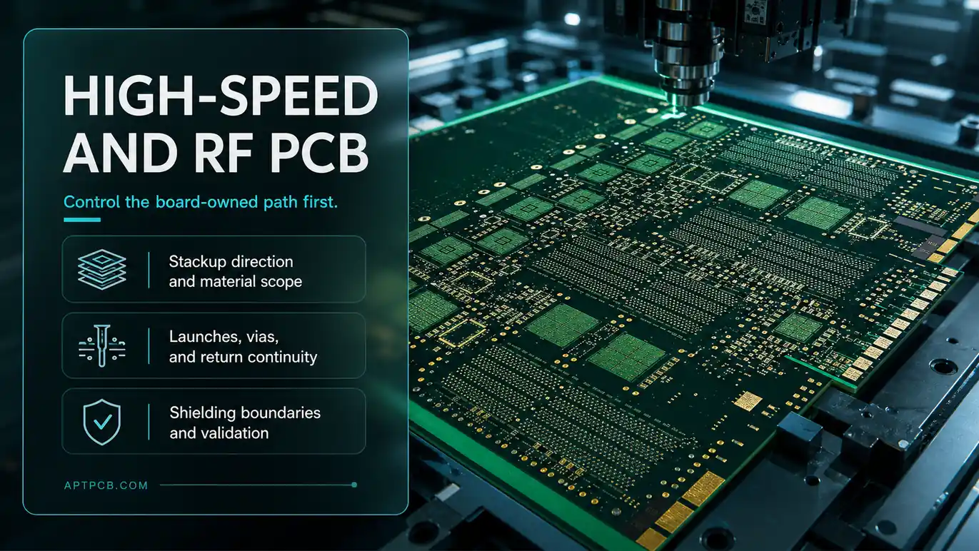
- The first risks usually appear where the board path becomes sensitive to stackup direction, material scope, local transitions, reference continuity, shielding boundaries, and staged validation.
- A 5G combiner board, a small-cell radio board, an antenna-tunable board, a low-noise RF front end, a PCIe Gen6 channel board, and an interference-sensitive mixed-signal board are not the same product type, but they often fail for similar release reasons.
- The safest engineering posture is to decide what part of the path the PCB actually owns, then review stackup, transitions, partitioning, and validation in that order.
Quick Answer
High-speed and RF PCB manufacturing becomes easier to control when the team separates board-owned path decisions from system-level claims. Start by confirming which layers and regions are truly performance-critical, then review stackup and material direction, local launches and via transitions, partitioning and shielding boundaries, and finally the validation evidence needed before pilot or production release.
If your first release questions already center on controlled structures, laminate choice, or loss-sensitive routing, start with PCB Impedance Control, High Frequency PCB, and PCB Stack-Up before using this guide to classify the deeper project-specific risk.
Table of Contents
- What counts as a high-speed or RF PCB here?
- What should engineers review first?
- Why stackup and material direction come first
- Why transitions, launches, and return paths create risk first
- How partitioning, shielding, thermal path, and enclosure context change the review
- Why validation must stay layered
- Which project types change the review order?
- What should be frozen before pilot or release?
- Next steps with APTPCB
- FAQ
- Public references
- Author and review information
What counts as a high-speed or RF PCB here?
Here, high-speed and RF PCB is a practical engineering umbrella for boards where signal path sensitivity changes the release order.
That includes, for example:
- 5G combiner boards
- 5G small-cell radio boards
- antenna-tunable boards
- low-noise RF front-end boards
- PCIe Gen6 or similar very-high-speed digital interconnect boards
- interference-sensitive mixed-signal boards with shielding or partitioning pressure
Those are different board families, but they often share the same release burden:
- the board path is no longer generic
- stackup and material choices are now tightly coupled to performance
- local transitions can consume margin early
- validation must be more layered and explicit
The focus here is board-level release readiness, not system compliance, field performance, or final application readiness.
What should engineers review first?
Start with these five boundaries:
- board-owned path
- stackup and material direction
- local transitions and return continuity
- partitioning, shielding, thermal path, and enclosure interaction
- validation ownership
That order matters because many weak high-speed or RF articles start with material branding or standards labels. In real projects, the more useful first question is simpler:
What part of the critical path is actually owned by the PCB, and what has to be frozen at board level before pilot release?
The first engineering questions are usually:
- Which lanes, feeds, launches, antenna regions, or mixed-signal corridors are truly performance-critical?
- Which layers really need lower-loss material, tighter impedance ownership, or more controlled transition design?
- Are the most sensitive failures likely to appear at local vias, launches, bends, splits, shielding edges, or enclosure-adjacent features?
- Is the board making claims that belong only to later RF, SI, EMC, or system validation?
- Does the release package clearly separate fabrication confirmation from later electrical, RF, or platform evidence?
Why stackup and material direction come first
Stackup is not only a drawing detail. In high-speed and RF work, it is one of the earliest indicators of whether the design is being released with the right physical assumptions.
The better question is not simply:
Do we need Rogers, Arlon, Megtron, Tachyon, or another premium family?
The better questions are:
- Which layers actually carry the performance burden?
- Can the design justify a hybrid material route instead of forcing premium material across the full stack?
- Does the stackup still read like a generic multilayer board while the real path is already more specialized?
- Are material notes aligned with routing length, reference structures, transitions, and later validation?
| Stackup question | Why it matters | Common release mistake |
|---|---|---|
| Which layers are truly critical? | Premium materials only help where the board path needs them | A premium laminate is applied too broadly or too vaguely |
| Is hybrid material strategy justified? | Hybrid routes can reduce cost without losing RF or SI intent | The board mixes materials without planning lamination and validation together |
| Are layer roles clear? | Controlled paths need stable references and explicit ownership | The stackup is frozen after routing assumptions are already drifting |
| Is material direction tied to actual path sensitivity? | Material names alone do not prove path integrity | A high-end laminate is used to compensate for an unresolved geometry problem |
For project-specific examples, see:
- 5G Combiner PCB Review: What Matters Before Release
- What to Check Before Releasing a 5G Small Cell PCB
- PCIe Gen6 SI Checklist for Mass Production
Each of those examples applies the same common rule in a different product context: material scope only matters when it matches board-path ownership.
Why transitions, launches, and return paths create risk first
Many high-speed and RF failures appear first at local discontinuities, not in the abstract block diagram.
That includes:
- connector launches
- BGA breakouts
- layer-change vias
- antenna feeds
- drilled transitions
- return-path interruptions
- shield boundary crossings
This is true across several seemingly different projects:
- a 5G combiner board can fail at RF transitions even when the laminate choice looks right
- an antenna board can become unstable when the feed and matching reserve are frozen too early
- a Gen6 board can sound electrically advanced while still leaving the most sensitive launch geometry vague
- an interference-sensitive board can lose margin because the return path breaks earlier than the signal trace review suggests
| Transition review area | Why it matters | What usually goes wrong |
|---|---|---|
| Launch geometry | Small discontinuities can consume margin before long routes do | The connector or pad transition is reviewed too late |
| Via strategy | Stub posture, return vias, and layer changes shape the local path | Through-via language is left generic while the path is already sensitive |
| Reference continuity | Return-current stability is part of the path | Signals are reviewed while the plane beneath them is not |
| Antenna handoff | Tuning path and feed ownership must stay measurable | The board is declared tuned before enclosure-aware retuning is finished |
For deeper examples of transition-sensitive designs, see:
- Antenna Tuning and Trimming: What to Lock Before Release
- PCIe Gen6 SI Checklist for Mass Production
- 5G Combiner PCB Review: What Matters Before Release
Across those cases, the common pattern is:
if the local transition is underdefined, the global performance story is already weaker than it sounds.
How partitioning, shielding, thermal path, and enclosure context change the review
High-speed and RF release discipline is not only about traces and laminate. Physical context matters.
The most common contextual pressures are:
- RF-sensitive and noisy digital or power regions sharing one board
- shield structures that affect both isolation and inspection access
- thermal density that changes behavior in compact enclosures
- mechanical surroundings that alter return paths, antenna tuning, or current flow
| Context pressure | What to review earlier | Why it changes the board decision |
|---|---|---|
| Mixed RF and digital regions | partitioning, zone ownership, return continuity | Functional regions start coupling before final system test |
| Shielding and fence-via features | closure method, rework access, probe access, finish zoning | Shield features affect assembly and validation, not only RF behavior |
| Compact radio node or small-cell enclosure | thermal escape path, nearby metal, service access | The enclosure becomes part of the board review |
| Interference-sensitive subsystem | board boundary versus system claim | The PCB should not overclaim immunity it cannot prove alone |
For detailed scenarios in these project types, see:
- What to Check Before Releasing a 5G Small Cell PCB
- Anti-Jamming PCB, Read as a Board Review
- RF Front-End Low Noise PCB Compliance
The governing rule stays the same:
board-level release claims must stay narrower than system-level performance claims.
Why validation must stay layered
One of the most common failures in high-speed and RF content is collapsing every evidence layer into one vague word: tested.
That is not enough.
| Validation layer | What it answers | What it does not prove |
|---|---|---|
| Fabrication and inspection evidence | Was the board built according to the intended route and quality gates? | Final RF, SI, EMC, or field performance |
| Impedance or coupon evidence | Does the board correlate with the controlled-structure intent? | Full application-level behavior |
| RF or SI measurement evidence | Do the measured paths behave acceptably in the scoped test setup? | Whole-system readiness in every environment |
| Compliance or platform validation | Does the board still perform acceptably in the real system context? | That earlier board-level evidence can be skipped |
This layered view matters because:
- a continuity pass is not RF proof
- a coupon pass is not platform proof
- a Gen6 launch correlation is not full-channel system proof
- a shielded board is not automatically an anti-jamming system
The project-specific deep dives are:
- RF Front-End Low Noise PCB Compliance
- Antenna Tuning and Trimming: What to Lock Before Release
- PCIe Gen6 SI Checklist for Mass Production
Which project types change the review order?
Different projects push different checkpoints to the top of the review.
| Project type | What moves to the top of the review | Deep-dive page |
|---|---|---|
| 5G combiner board | RF-critical laminate scope, return continuity, transition control, finish zoning | /en/blog/5g-combiner-pcb |
| 5G small cell board | compact-node stackup, RF coexistence, thermal path, enclosure interaction | /en/blog/5g-small-cell-pcb |
| Antenna-tunable board | antenna-region discipline, matching reserve, enclosure-aware retuning | /en/blog/antenna-tuning-and-trimming |
| Low-noise RF front-end board | low-noise path ownership, staged compliance evidence, grounding posture | /en/blog/rf-front-end-low-noise-pcb-compliance |
| PCIe Gen6 board | path ownership, stackup and material direction, local launches, via posture | /en/blog/pcie-gen6-si-checklist-mass-production |
| Interference-sensitive mixed-signal board | partitioning, shielding, return continuity, board-vs-system boundary | /en/blog/anti-jamming-pcb |
That table helps the reader classify the project and then follow the most relevant deep-dive path.
What should be frozen before pilot or release?
Before pilot or production release, freeze the decisions that change the board path and its evidence boundary:
- the board-owned critical path
- stackup direction and material scope
- launch, via, and return-path intent
- partitioning, shielding, and enclosure-linked assumptions
- the validation layers required before pilot, production, or system handoff
- the boundary between board proof and later platform or compliance proof
If those items are still moving, the project may still be buildable, but it is not yet a clean high-speed or RF release package.
Next steps with APTPCB
If your high-speed or RF PCB program is being slowed by unresolved stackup direction, unclear material scope, unstable local transitions, shielding-access conflicts, or confusion between board validation and system proof, send the Gerbers, stackup targets, material notes, and validation expectations to sales@aptpcb.com or upload the package through the quote page. APTPCB's engineering team can review whether the real release risk sits in board-path ownership, fabrication-route complexity, or evidence layering before pilot build.
If the package still needs front-end cleanup, review:
FAQ
Is a high-speed PCB the same as an RF PCB?
Not necessarily. They are different application families, but both often demand tighter control of stackup, transitions, references, and validation scope.
Is premium laminate enough to make a board high-speed or RF-ready?
No. Material choice only helps when it matches the actual board-owned path, stackup direction, and local transition design.
Where do high-speed or RF boards usually fail first?
Often at local discontinuities such as launches, vias, return-path breaks, shield boundaries, or antenna-region handoffs rather than at the longest visible trace.
Does a tested board automatically prove RF or SI readiness?
No. Fabrication evidence, impedance evidence, RF or SI measurement, and system-level validation answer different questions.
What is the safest way to release a high-speed or RF board?
Freeze path ownership, stackup direction, material scope, local transition intent, and validation boundaries before pilot or production release.
Public references
APTPCB PCB Stack-Up
Supports stackup planning and controlled-structure review context.APTPCB PCB Impedance Control
Supports controlled-impedance handoff and validation direction.APTPCB High Frequency PCB
Supports RF-oriented board-family context.APTPCB HDI PCB
Supports advanced interconnect and build-up routing context.APTPCB DFM Guidelines
Supports manufacturability review as an intake gate before release.
Author and review information
- Author: APTPCB high-speed and RF content team
- Technical review: stackup, CAM, SI, RF, and release engineering team
- Last updated: 2026-05-08