
In a conventional rigid multilayer PCB, a core is a cured laminate, usually supplied with copper on one or both faces. Prepreg is reinforcement impregnated with partially cured resin. During lamination, the prepreg bonds neighboring layers and becomes part of the finished insulation. The two materials work together; choosing one does not eliminate the need to design the complete stackup.
The distinction becomes practical when a drawing calls for a particular dielectric spacing, finished thickness or impedance. A prepreg sheet before pressing is not automatically the same thickness as its finished dielectric layer. Ask for the proposed pressed construction, then check it against the electrical, mechanical and procurement requirements of the board.
For a broader view of laminate families, see what copper-clad laminate is. The PCB stackup design article addresses the larger layer-order and design problem. Here the focus is the material between those layers and what to confirm before releasing it.
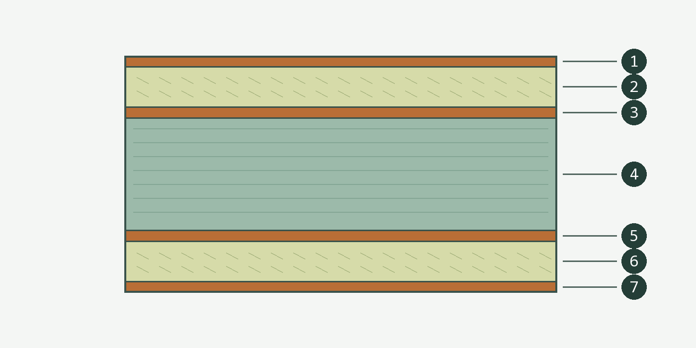
The cross-section is a conceptual foil construction, not a fabrication drawing or a scale image. The outer copper layers are 1 and 7, prepreg regions are 2 and 6, inner copper layers are 3 and 5, and the central cured core is 4. The finished properties depend on the actual materials and process.
What is the difference before pressing?
For a common rigid-board construction, the core starts as a cured dielectric laminate with bonded copper. A fabricator can image and etch that copper to form inner-layer circuitry before building it into a multilayer stack. “Core” describes its role in the construction; it does not identify the resin system, guarantee a particular thickness or mean that every board uses the same number of cores.
Prepreg means pre-impregnated reinforcement. In the glass-reinforced thermoset materials discussed here, the fabric carries resin that has been partially cured. It is assembled between neighboring surfaces and processed under heat and pressure. The resin flows and cures as the stack is bonded. The Isola 370HR Processing Guide describes the received prepreg and the fully cured laminate for that particular material family; other materials and bonding systems require their own documentation.
Calling prepreg “glue” is useful shorthand, but incomplete. The material also becomes part of the dielectric between conductive layers. Its composition and finished geometry matter to electrical and mechanical design. Equally, “core” is not a synonym for copper: the dielectric and its copper cladding are different parts of the laminate.
| Question | Cured core | Prepreg before lamination |
|---|---|---|
| What arrives for the build? | Cured laminate, commonly copper clad; the copper can be patterned for an inner layer. | Reinforcement carrying partially cured resin, supplied as bonding material. |
| What does it contribute? | A defined laminate construction and, where clad, a surface for circuitry. | Bonding and dielectric material between adjacent surfaces after pressing. |
| What should a designer confirm? | Material identity, dielectric construction, copper and supplied thickness. | Material identity, ply construction, finished dielectric thickness and compatibility with the build. |
| What does the name alone prove? | Neither final board thickness nor product qualification. | Neither pressed thickness, finished impedance nor the absence of voids. |
These descriptions concern common glass-reinforced rigid multilayers. Flex constructions, metal-base boards and specialty bonding films can use different materials or terminology. Ask for the actual construction instead of forcing those products into this simplified model.
Reading a four-layer construction
In the illustration, layers 3 and 5 are the copper faces of a central core. After the inner copper is patterned, prepreg is placed outside it and copper foil is added on each side. The stack is laminated into one board. A finished four-layer PCB therefore has four conductive layers even though the material descriptions also count cores, prepreg plies and foil.
There can be more than one prepreg sheet in one dielectric region. A drawing that lists “two plies” identifies a construction choice; it does not mean that either ply retains its original nominal thickness in the finished board. Nor does it mean that all four-layer boards must use the construction shown. Layer order, copper distribution, material availability and the fabricator's process all affect the proposed build.
When reviewing a stackup, follow the copper layer numbers from top to bottom. Identify the dielectric between every pair and distinguish the finished copper thickness from the starting foil where plating or processing changes the outside layers. For controlled structures, identify the actual signal layer and its reference layer. A total thickness alone cannot tell you how far a trace is from its reference plane.
Why is pressed thickness a separate requirement?
Prepreg resin must bond neighboring surfaces and accommodate the copper features within the stack. The finished dielectric is affected by material construction, resin flow, the adjacent copper pattern and the selected lamination process. A number taken from an unpressed sheet listing is therefore not a dependable substitute for an agreed pressed stackup.
Consider a hypothetical board with an overall thickness requirement set by its enclosure and a controlled signal on an outer layer. The designer receives a proposed stackup with the correct overall thickness, but the dielectric under that signal is thicker than assumed in the original routing. Both drawings may say “four layers,” yet the signal geometry is no longer the same. The appropriate response is to review the actual stackup and impedance calculation with the fabricator, not to assume the board is acceptable because its total thickness matches.
The reverse is also possible: the local spacing may meet the electrical design while the sum of the finished layers does not meet the mechanical requirement. Ask the fabricator which values are nominal, which tolerances are offered and how they will be verified. Board thickness, individual dielectric thickness and impedance are related but distinct acceptance questions.
Do not calculate a final layer by adding nominal unpressed ply values and treating the sum as a guaranteed result. That arithmetic can be an early estimate, but it cannot model the actual press, copper fill, resin flow and other construction details. The approved manufacturing stackup is the appropriate handoff for a specific order.
What does material choice mean for impedance and loss?
The impedance of a trace depends on its geometry and surrounding dielectric, including trace width, copper thickness, spacing to reference conductors and the dielectric properties used in the calculation. A core/prepreg label by itself is not an impedance target. Prepreg is not automatically unsuitable for controlled impedance, and a cured core does not automatically guarantee it.
Material datasheets are useful inputs, but their dielectric constant and loss values must be read with the stated frequency, method and construction. For example, the Isola 370HR data sheet, Revision E, lists a typical dielectric constant of 4.17 at 1 GHz, measured using IPC-TM-650 2.5.5.9. That is a conditioned example for the named product, not a universal value for FR-4, a design value for every stackup or proof of a finished PCB's impedance. Request the data appropriate to the proposed construction and the calculation method used for the job.
If the project specifies controlled impedance, mark the relevant traces or nets, target and tolerance, reference layers, and any agreed measurement or coupon requirement. The impedance-controlled PCB article goes further into the electrical handoff. Passing an agreed coupon check helps assess the specified structure; it does not by itself validate every channel, connector or complete system.
Loss is another distinct question. Two materials with a similar dielectric constant may have different loss behavior, and copper foil and conductor geometry also matter. If a channel has a loss budget, agree on the applicable material data, structure and validation approach with the design and fabrication teams. Do not assume a core is always lower loss than prepreg simply because its resin was cured earlier.
Do the core and prepreg have to be the same material?
They need to form an appropriate, manufacturable construction; that does not mean the drawing can safely name any two products and assume they are compatible. A material family may offer both laminate and prepreg intended to work together. Some designs combine different material systems, but the proposed combination and its processing need review for the particular build.
Start with the properties the product actually needs. The FR-4 material properties article explains why Tg, decomposition behavior, dielectric properties and other data cannot be reduced to a single grade name. In a mixed construction, also ask which dielectric sits next to each critical signal, what copper foil is proposed, and whether the material combination affects the fabrication sequence or qualification plan.
A supplier's proposed equivalent is a change request, not merely a spelling change. Compare the exact laminate and bonding materials, their relevant datasheets, the revised stackup and the effect on controlled features. The design authority should decide whether additional analysis, samples or product testing are needed. Similar Tg values alone do not establish equivalence, and an approved alternative for one product is not automatically approved for another.
A practical review before approving the stackup
Suppose an engineer requests a thin four-layer board for a connector and needs controlled impedance on selected nets. A purchaser receives two proposals with the same finished board thickness. One identifies the core, dielectric regions and impedance structures; the other only says “FR-4, four layers.” They are not yet equivalent descriptions of the build.
First, reconcile the board thickness and tolerance with the connector and enclosure drawings. Then compare the material and layer table against the design: which copper layers are signals, which are references, and what finished dielectric spacing is proposed for each controlled structure? Check whether the impedance target, tolerance and agreed verification are included in both quotations. Finally, establish whether an alternate material or change in ply construction needs written approval before production.
This is a hypothetical review, not a measured build or customer case. Neither proposal should be accepted or rejected from the short descriptions alone. The missing information is a reason to ask questions, not proof of a defect or a forecast of cost.
| If the proposal says... | Clarify before release |
|---|---|
| “FR-4 or equivalent” | Which laminate and prepreg are proposed, which properties matter, and who approves substitutions? |
| “Four layers, specified total thickness” | What are the layer order, finished dielectric spacings, copper assumptions and tolerances? |
| “Controlled impedance” | Which nets and reference layers, target and tolerance, coupon or other agreed verification, and report scope? |
| “Two prepreg plies” | Which construction and expected pressed thickness are proposed for this copper pattern? |
| “Same as the last order” | Which approved revision, material construction and change-control record does that refer to? |
For a quotation or stackup discussion, provide the layer order, fabrication data and drawing, finished board thickness and tolerance, copper requirements, controlled nets and any material or approval constraints. The fabricator can then review feasibility and propose a construction; the product team remains responsible for system-level qualification. Use PCB fabrication services for related manufacturing context, request a project-specific quote, or contact the team to clarify the handoff.
What should be kept with the released files?
Keep the approved stackup revision with the fabrication drawing and design files, and identify which document controls if there is a conflict. The record should show the material designations, layer sequence, relevant dielectric and copper assumptions, finished thickness, controlled-impedance requirements and approved substitutions. Agree separately on inspection evidence and retention where the project needs it.
If the design or supply changes, compare the new proposal with the approved revision before building. A change in prepreg construction may affect several requirements at once: local spacing, overall thickness, material availability and the analysis used for an impedance calculation. Review those effects together and record the decision, rather than changing one row of a spreadsheet without checking the rest of the board.
For the underlying materials, consult the material manufacturer's current datasheet and processing documentation for the exact product. A fabricator's proposed stackup and order-specific agreement define the build to be reviewed; neither a generic article nor a datasheet alone is a finished-board acceptance plan.