
Two traces in a differential pair can be the same length and still have different propagation delays. One possible contributor is the glass weave effect: the conductors pass through slightly different local dielectric environments in the laminate. Over a long route, that difference can contribute to timing skew between the pair's positive and negative signals.
The effect is worth evaluating when the interface has a tight timing budget. It is one possible cause of skew, not a conclusion to draw from a single failed measurement. Package paths, connectors, vias and routing asymmetry also need attention.
How a woven laminate can affect a signal
Many PCB laminates use woven glass fabric in a resin system. The glass-rich bundles and resin-rich spaces have different dielectric properties. A trace does not interact with only one tiny point in the material, but local variations in the composite can change its effective propagation environment.
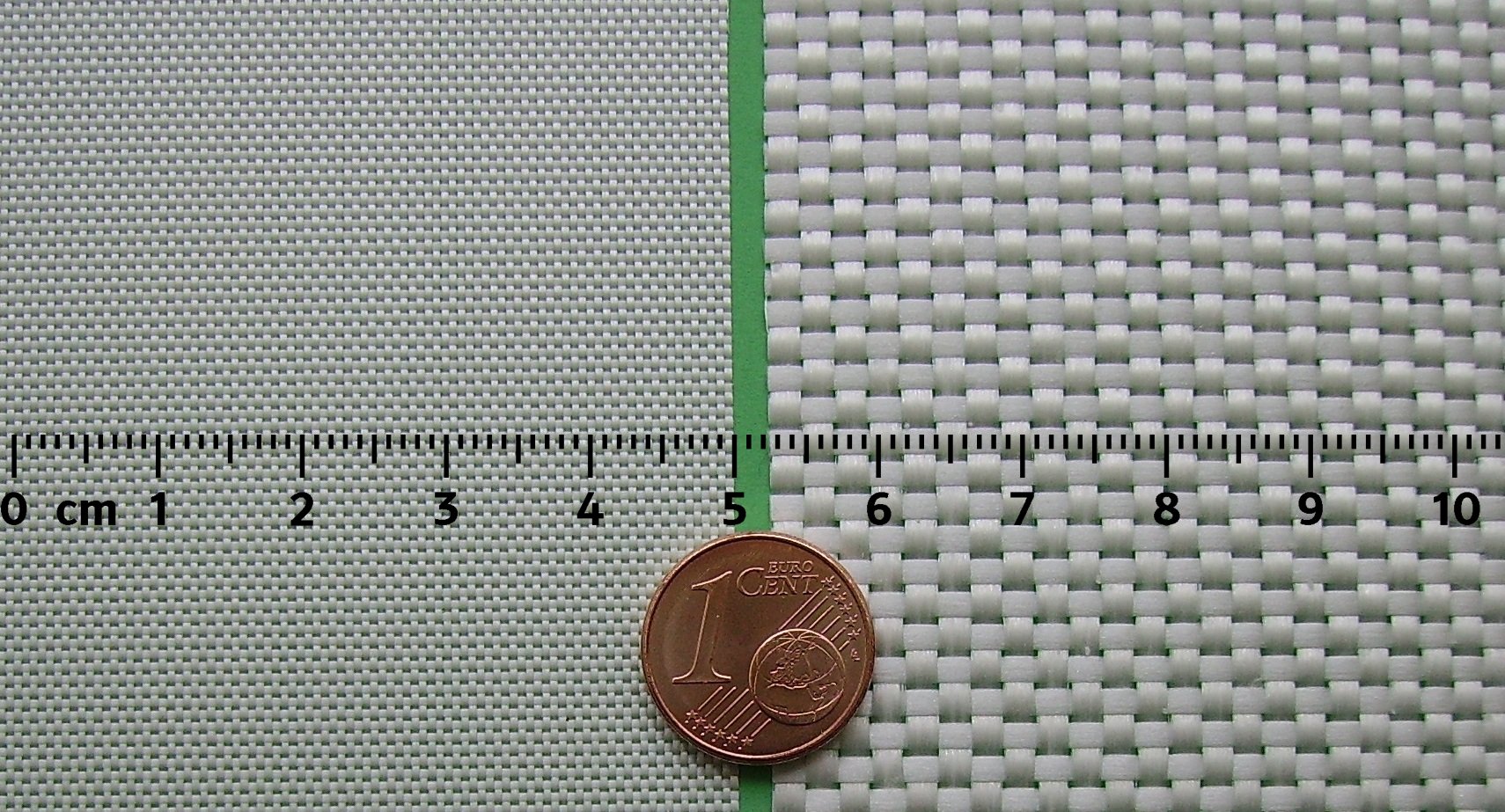
Two glass fabrics used as reinforcement in composites. They illustrate differences in weave; the photo does not identify PCB fabric styles or a finished laminate.
If two nearby conductors encounter those variations differently along their lengths, their accumulated delays can differ. The result depends on the actual dielectric construction, trace geometry, relationship to the weave, routing direction and other features of the channel. The dielectric constant guide explains the broader material property; a bulk datasheet value alone does not describe every local region under a route.
Why orientation and construction matter
Consider a pair whose long section runs close to one direction of a woven fabric. Depending on registration between the traces and the fabric, the two conductors may encounter different proportions of glass-rich and resin-rich regions. Changing the path angle changes that relationship along the route; it does not remove every other contributor to delay.
The fabric is only part of the stack. The dielectric above and below a signal layer, the number and arrangement of plies, conductor geometry and reference structures influence the actual electromagnetic environment. For that reason, ask about the proposed pressed construction on the critical layer rather than selecting a fabric style from a list in isolation.
Two boards with the same outline can also have different relationships between artwork and fabric if the manufacturing panel or material is oriented differently. If the design depends on an orientation assumption, put that assumption in the handoff and have it confirmed.
Keep length, skew and impedance separate
Length matching is a layout check. Intra-pair skew is the difference in delay between the two members of one pair. Inter-pair skew compares separate pairs. These are related checks, but they are not interchangeable.
Similarly, a differential impedance coupon answers a different question from a P/N delay measurement. A result within the specified impedance range does not establish that the complete channel meets its timing budget. The differential pair routing guide covers the wider set of layout decisions, including reference planes and transitions.
| Observation | What it tells you | What to check next |
|---|---|---|
| P and N have matching drawn lengths | One geometric source of mismatch has been addressed. | Check delay contributions from routing, construction, packages and connectors. |
| Differential impedance passes on a coupon | The tested structure met that impedance requirement under the stated test conditions. | Check timing separately on structures representative of the critical channel. |
| P/N delay differs on a measured route | The measured channel has a delay difference at the chosen reference planes. | Compare other routes, geometry, fixtures and constructions before attributing a cause. |
Set a timing requirement before choosing a mitigation
Find the requirement in the applicable device and interface documentation and establish the reference planes. Determine whether the specified limit applies to the board alone or to a larger channel that includes packages, connectors and other structures. A board layout rule can only be useful when it fits that complete requirement.
Record the allowed P/N skew at those reference planes and identify which parts of the channel are included. Track estimates and uncertainty for the board geometry, material, launches and any package or connector contributions within that boundary. Contributions can have different signs; cancellation in one nominal estimate does not guarantee margin across manufacturing variation. Use the interface documentation and an agreed worst-case or statistical method for the actual design.
Why one coupon position can be misleading
Compare representative structures at multiple positions where the investigation warrants it, and record their orientation and construction. A single coupon that happens to sample a favorable registration can hide variation elsewhere; conversely, a single unfavorable result does not establish the distribution for all panels.
Options to discuss with the fabricator
There is no universal angle or glass style that solves every channel. Compare candidate changes against the actual stackup and timing requirement:
| Candidate action | Potential purpose | Tradeoff or question to resolve |
|---|---|---|
| Specify a spread-glass construction | Reduce local nonuniformity in the proposed dielectric | Is the exact material and pressed construction available, and what evidence supports it? |
| Adjust route angle or panel orientation | Change how the route crosses fabric features | Does it fit the layout and panel, and what is the angle relative to the actual weave? |
| Change the dielectric ply arrangement | Explore a different effective construction | How do final thickness, impedance, lamination and available material change? |
| Change pair geometry | Meet the combined routing and electrical requirements | Does the revised pair still meet impedance, spacing and other layout constraints? |
These actions are not independent switches. A change to the dielectric construction can require an impedance review, and a routing change can affect length, space and transitions. Ask the fabricator and signal-integrity team to compare complete candidates and confirm available constructions and substitution controls. The core and prepreg guide explains how these stackup elements fit together.
A hypothetical investigation
A design team has a long high-speed differential pair. Its CAD tool reports equal routed lengths, but a prototype measurement shows unequal P/N delay. Before changing the laminate, the team checks the measurement reference planes and fixture, then reviews connector and package contributions, breakout geometry, vias and asymmetrical sections of the route.
If material variation remains a concern, the team can plan representative test structures on the relevant layer and construction. A comparison can help investigate a possible weave contribution; one coupon or one skew number does not establish a universal material property or prove the cause of a channel failure. See PCB test coupons for broader coupon planning.
Turn the investigation into a measurement plan
- Define the question. Decide whether the immediate concern is the complete channel, a board-only allocation or a comparison between proposed stackups. Set the relevant reference planes and acceptance requirement.
- Choose representative structures. Identify the critical layer, conductor geometry and construction. Plan comparisons at more than one location and orientation where practical, including structures that help separate material effects from known geometric differences.
- Record the build. Preserve the material and ply information, layer, panel position and orientation relative to the fabric when available. Note any approved substitutions.
- Document the measurement. Specify equipment bandwidth, fixture, calibration or de-embedding and delay-extraction method. Record P/N delay and differential impedance separately, together with the reference planes.
- Compare and investigate. Look for differences across the planned structures and builds. Review layout, launches, test setup and material construction before assigning a cause. Decide whether additional channels, panels or lots are needed for the project's decision.
A test structure can support an investigation without being a complete model of every route. Document where it differs from the product channel, particularly at breakouts, transitions and connectors.
What to include in the handoff
Send the interface requirement and the portion of its timing budget allocated to the board. Identify the critical pairs and layers, approximate routes, impedance requirements, proposed stackup and any constraints on routing direction. Ask the fabricator to confirm the material and prepreg construction, available cloth information, panel orientation and substitution controls.
Agree on whether representative structures, measurement data or additional verification are needed before release. If a construction change is proposed, review its effect on the other requirements as well, including thickness, impedance and availability. Our PCB material selection guide covers the wider tradeoffs.
To discuss a specific stackup and its available options, request a quote or contact APTPCB.