
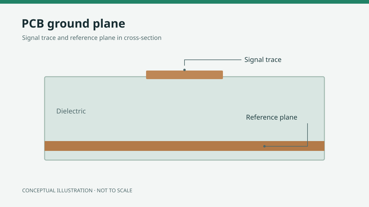
A useful PCB ground plane gives signals an intentional, continuous reference and a practical path for return current. Start by assigning reference planes in the stackup, route critical signals over continuous copper, and inspect what happens at splits, connectors and layer transitions. A ground-net label alone does not guarantee continuity: check the actual copper and the complete current loop.
The right solution depends on the signal, stackup, device requirements and isolation boundaries. A plane can help control return-path geometry, but it does not automatically solve EMI, crosstalk, power integrity, ground loops or safety.
What a ground plane does
A ground net is an electrical connection defined in the design. It tells the layout tool which pads, vias and copper belong together. A ground plane is a conductive layer or region used as a reference and return-current path. A copper pour is a tool-generated copper region assigned to a net; it may form a useful plane, but its usefulness depends on the copper that remains after clearances, cutouts and connections are applied.
For example, a pour assigned to ground can contain narrow necks, isolated islands or gaps around other features. The net name may be correct while a signal’s return path is still indirect. Conversely, two areas visually close to each other are not necessarily connected or intended to share a net.
Every signal current must complete a loop through a return path back toward its source. The distribution of that return current depends on frequency and geometry:
- At lower frequencies, resistance is often an important influence, and current can spread across available conductors.
- As frequency rises, inductance and the geometry between a signal and its reference become more influential. Return current tends to concentrate closer to the signal’s path where a suitable reference exists.
- A real waveform contains a range of frequency components, so it is misleading to assume that all return current always travels directly underneath a trace.
Provide a suitable reference and inspect where the loop must travel, especially where the geometry changes. Adding ground copper alone does not resolve those paths.
Plan the stackup around signal references
Before routing, identify the layers that will carry important signals and the conductive layers intended to reference them. For each signal layer, ask:
- Which plane or copper region is its reference?
- Is that reference continuous along the intended route?
- What happens when the signal changes layers or enters a connector?
- Are there regions where copper clearances, cuts or isolation boundaries interrupt the reference?
A signal layer adjacent to a continuous reference plane can make this review easier because the relationship between the route and its reference is visible in the stackup plan. But the layer assignment is only a starting point: the finished layout can still introduce gaps, voids and transitions that change the return path.
Use the layer plan to protect important reference areas before lower-priority routing consumes them. Review high-speed interfaces, sensitive analog paths, clocks and other signals identified by the device or system design as critical. Their needs may differ, so do not assume one routing treatment is sufficient for every class.
The articles on PCB stackup design and PCB layers explained provide related layer-planning context.
Before release, use the PCB layout DFM guidelines to review manufacturing constraints alongside the reference-layer plan.
Keep the actual reference copper continuous
A plane can be interrupted by intentional splits, board slots, mounting features, connector clearances, via clearances and dense routing. A signal crossing one of these interruptions may force its return current to find a longer or different route. That can enlarge the current loop and change coupling to nearby structures.
When inspecting a crossing, look beyond the trace itself:
- Display the signal layer and its intended reference together.
- Check the shape of the reference copper on both sides of the crossing.
- Look for narrow connections or disconnected copper created by clearances.
- Trace a plausible return path back toward the source rather than judging the gap in isolation.
- Check whether a proposed reroute creates a different problem elsewhere.
Avoid crossing a reference interruption when a suitable continuous path is available. If the crossing is necessary, determine how the return path is provided and whether the design constraints allow it. An intentional isolation barrier is not an ordinary plane gap to be patched over.
Inspect antipads and dense via fields
An antipad is a clearance in a plane around a feature that must not connect to that plane. Individual antipads may be necessary, but several neighboring clearances can combine into a slot or remove a large portion of the reference copper.
This is particularly worth checking near dense connectors and layer-transition areas, where many vias may be close together. Review the resulting copper shape after the clearances are applied, not just the nominal plane outline. If the remaining copper interrupts a critical return path, consider whether the routing, pin escape or via arrangement can be changed within the design and manufacturing constraints.
Handle layer transitions as return-path transitions
A signal via moves a route from one layer to another. It may also change the signal’s reference, even if the schematic shows no change in net. Review the reference on the entry layer and the reference on the exit layer as part of the same transition.
When both references are on the same ground net
If the signal moves between layers referenced to different plane layers on the same ground net, the return current needs a connection between those plane layers. A nearby same-net stitching via can provide a path between them, provided it connects to the intended copper on both layers and the surrounding geometry remains suitable.
This is not a reason to place vias mechanically at every transition. Check the actual plane connections, clearances, other nearby vias and the signal’s route. A via that appears nearby in a top view is not useful for this purpose if it does not connect the relevant reference copper.
PCB via stitching covers the related role of vias in connecting same-net copper.
When the references are at different potentials
If the signal moves between layers referenced to different-potential planes, a same-net ground stitching via does not by itself connect the two references. The transition requires a deliberate return-path review that accounts for the circuit, plane coupling and device guidance.
Do not add a connection or capacitor as a universal fix. Its suitability depends on the reference nets, the frequency-dependent path, the surrounding power distribution and the application. Consult the relevant device datasheets and design constraints, then validate the chosen transition as part of the system.
When an isolation boundary is involved
Galvanically isolated domains require separate treatment. Do not short isolated grounds together or bridge a safety barrier to make a return path appear continuous. Components and conductive structures across a barrier may be restricted by the isolation design and applicable safety rules.
Identify where a signal is intended to cross the boundary, what isolation method the circuit uses, and which clearances and other requirements apply. If the route cannot meet those constraints, escalate the issue to the circuit and safety design owners rather than treating it as a routine plane-stitching problem.
Include connectors in the return-path review
A clean route across the PCB is only part of the loop. At a connector, examine how the signal and its return path leave the board, how they relate to the connector pin assignment, and what happens on the other side when that information is available.
A connector’s ground pins may be assigned to the correct net but still connect through constrained copper, a dense antipad field or a path shared with unrelated current. Conversely, a board-level view may not reveal the full return path through a cable or mating assembly.
For critical interfaces, coordinate connector pinout and escape routing with the system design. Review the reference copper up to the connector, the ground connections that are intended to support the interface, and any domain boundary at the connection. Do not assume that a ground pin automatically makes every adjacent signal path acceptable.
Mixed-signal placement: manage current paths, not labels alone
Mixed-signal boards can contain sensitive analog circuitry alongside digital switching and power conversion. The first decisions are often functional: place related components so that their signal and return-current paths are understandable, and keep disruptive current loops from unnecessarily crossing sensitive regions.
A continuous ground plane can be a good starting point because it avoids forcing signals across deliberate splits. However, continuity alone does not prevent a noisy return current from sharing an undesirable path. Placement, routing, connector location and power-current loops still matter.
Likewise, splitting ground copper is not a universal way to protect analog circuitry. A split can redirect current, but it can also create an interruption beneath a signal that must cross between regions. Some devices specify particular grounding, layout or connection arrangements; follow their datasheets and evaluate those instructions in the context of the complete board.
For each mixed-signal interface, identify:
- The source and destination of the signal and its return.
- Nearby switching or power-current paths.
- Whether the signal crosses a plane boundary or changes reference.
- The grounding and placement requirements of the connected devices.
- Whether an intentional isolation boundary changes the permitted connections.
Neither a split plane nor a continuous plane guarantees acceptable noise or EMC performance. The decision must be supported by the actual current paths and the validation appropriate to the product.
Hypothetical route inspection
Hypothetical example: A designer is reviewing a digital interface routed from a controller to a connector. The first part of the route runs on a signal layer referenced to a ground plane. Near the connector, the trace crosses a gap in that plane caused by a copper-region boundary. The trace then changes layers and continues on a layer referenced to another plane layer on the same ground net.
The designer performs two separate checks:
- Reference gap: With the trace and reference copper displayed together, the designer confirms that the trace crosses the gap. The preferred layout investigation is to reroute the trace over continuous reference copper or revise the copper arrangement if the circuit and other constraints permit. The designer also checks the connector escape so that the reroute does not simply move the interruption closer to the pins.
- Layer transition: At the signal via, the designer checks that both reference planes belong to the same ground net and that there is a suitable connection between them. A nearby stitching via is considered only after confirming that it can connect the intended copper on both layers without creating another clearance problem.
The two fixes address different discontinuities. A stitching via at the layer change does not automatically repair the earlier reference gap. If the gap represented an isolation boundary instead, joining the copper would not be an acceptable routine fix; the boundary and crossing would need to be reviewed against the isolation design.
After the layout change, the designer repeats the continuity inspection and passes the relevant interface and transition information to the validation owner. The example illustrates a review method, not a prediction that the product will meet an EMI or signal-integrity target.
Troubleshooting and review decisions
| Symptom or observation | Layout check | Decision and validation |
|---|---|---|
| A critical trace crosses a plane split or slot | Overlay the trace with its reference copper and identify the return path around the interruption. | Investigate rerouting over continuous reference or revising the copper region. Preserve intentional isolation and validate the resulting interface. |
| A signal changes layers | Identify the reference on each layer and inspect the copper and connections around the signal via. | For same-net references, assess an appropriate stitching connection. For different potentials, review the transition with the circuit and device constraints. |
| A connector area has many clearances | Inspect antipads and the remaining reference copper, including paths to intended ground pins. | Consider changes to pin escape, routing or via arrangement; coordinate with the connector and system design. |
| A copper pour is assigned to ground but looks fragmented | Check islands, narrow necks, net assignments and connections after the pour is generated. | Correct unintended fragmentation where permitted, then inspect critical return paths again. |
| Analog behavior is sensitive to nearby switching | Map functional placement and the signal, power and return-current loops. | Rework placement or routing based on the observed paths and device guidance; validate rather than assuming a plane split will cure the issue. |
| A route approaches an isolated-domain boundary | Check the intended crossing method, domain nets and applicable barrier constraints. | Escalate to the circuit and safety owners. Do not bridge the barrier as a plane-continuity fix. |
| EMI or crosstalk remains a concern despite a ground plane | Review return continuity along with routing, coupling, connectors and other relevant system paths. | Select measurements or analysis appropriate to the concern; a plane by itself is not evidence of a pass. |
Prepare the design handoff
Before releasing the layout, document its assumptions and unresolved decisions. Include:
- Stackup, plane and net map: Identify signal layers, reference layers, plane regions, net assignments and intentional gaps.
- Critical signal classes: List the interfaces and sensitive paths requiring review, along with applicable device constraints.
- Layer changes and gaps: Identify transitions, reference changes, splits, slots, connector escapes and significant clearance-driven interruptions.
- Isolated-domain boundaries: Mark the boundary, intended crossing method and constraints that prohibit or control connections across it.
- Open decisions: Record any return paths that could not be confirmed and the owner responsible for resolving them.
- Measurement or simulation plan: State what will be evaluated, by whom, and against which project requirements. Use analysis and test results to support decisions, not as an assumed guarantee.
- Signoff ownership: Name the project roles responsible for layout approval, manufacturing review and system validation.
The PCB designer owns the layout intent: net assignments, reference choices, routing and the documentation needed to review them. The fabricator reviews and processes the supplied manufacturing information within the agreed manufacturing scope; that processing does not establish signal integrity, EMC compliance or finished-product qualification. The system-validation owner determines and carries out the relevant product-level checks and coordinates resolution of failures.
The Gerber file guide explains the artwork used for fabrication. When the board is ready for a manufacturing discussion, send APTPCB the Gerbers, stackup, intended reference layers and fabrication requirements. Include any requested reviews or tests so their scope can be agreed. Request a quote or contact APTPCB.
For further design context, consult Texas Instruments’ PCB Design Guidelines for Reduced EMI and High-Speed Layout Guidelines, and Analog Devices’ What Are the Basic Guidelines for Layout Design of Mixed-Signal PCBs? Apply their guidance alongside the specific device datasheets and the requirements for the product under review.