Millimeter-wave frequencies begin at 30GHz and extend to 300GHz. In that range, a physical board stops behaving the way a circuit schematic predicts it will. A via transition that's an ideal short circuit at 10GHz is a resonant structure with measurable inductance and a frequency-specific reflection at 77GHz. A surface roughness that's irrelevant at microwave frequencies adds 30–40% more conductor loss at millimeter-wave. A ground plane gap that goes unnoticed at 5GHz launches a surface wave that corrupts a 60GHz antenna pattern.
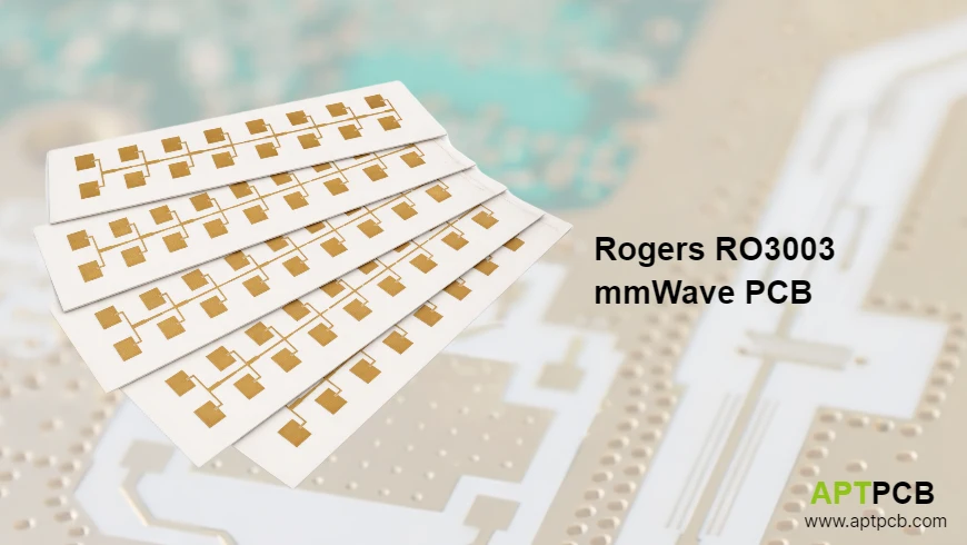
This article is about what changes physically when frequency crosses into the millimeter-wave band, and what those changes require of the PCB substrate, the trace geometry, the via structures, and the fabrication process. Rogers RO3003—with Dk 3.00 ± 0.04, Df 0.0010, and TcDk −3 ppm/°C—is the substrate around which most commercial mmWave PCB design is built. Understanding why requires understanding the physics that makes other materials inadequate.
The Millimeter-Wave Physical Environment on a PCB
Three physical effects, all of which scale with frequency, become dominant above 30GHz and drive the material and geometry requirements for mmWave PCBs:
Effect 1: Skin Depth Approaches Conductor Roughness
Skin depth in copper follows δ = 1 / √(π × f × μ × σ). At 77GHz, this works out to approximately 0.24 μm. Standard electrodeposited copper has RMS surface roughness Ra ≈ 5–7 μm—twenty to thirty times larger than the skin depth. Current is forced to follow the contours of the rough surface, effectively traveling a longer path than the straight-line trace length. The result is 30–40% more conductor loss than a flat surface would produce.
Low-profile ED copper (Ra ≈ 1.5 μm) reduces—but does not eliminate—this penalty at 77GHz. The ratio of roughness to skin depth is still approximately 6:1. The conductor loss premium over ideal smooth copper is approximately 10–15% with low-profile foil, versus 30–40% with standard foil. For a 3-inch transmit feed network, that difference is measurable—and it's why low-profile copper is the standard specification for mmWave RO3003 programs, not an upgrade option.
This is a laminate-level specification: it must be defined when the Rogers material is ordered, not addressed during or after fabrication. APTPCB sources all mmWave RO3003 programs with low-profile ED copper or RTF (Reverse Treated Foil) as standard.
Effect 2: Via Dimensions Approach Resonant Structures
At low frequencies, a through-hole via connecting a microstrip trace to an inner layer or ground plane is modeled as a lumped inductance—small, predictable, easily compensated. At millimeter-wave frequencies, the physical dimensions of a via approach the electrical quarter-wavelength. A 0.3mm via in a 1.6mm board has a stub length that resonates at approximately 46GHz in air (considerably lower when surrounded by dielectric). For a 77GHz design, this stub resonance falls within the operating band and creates a transmission null—a complete loss of signal at a specific frequency.
The solutions are: blind vias (connecting only to the layer they need to reach, with no stub below), back-drilling (removing the stub portion of a through-hole via with a slightly larger drill), or minimizing stub length through stackup design (placing signal layers near the board surface). All three require deliberate design—they don't happen by default.
Effect 3: Surface Wave Modes Become Active
In a microstrip structure, the dominant transmission mode is a quasi-TEM wave guided by the trace above the ground plane. At high frequencies, the dielectric substrate also supports surface wave modes—waves that propagate laterally within the dielectric rather than along the trace. These surface waves radiate at dielectric boundaries, couple into adjacent traces and antenna elements, and corrupt the antenna radiation pattern.
The substrate dielectric constant determines the cutoff frequency for surface wave mode excitation. Lower Dk substrates have higher cutoff frequencies—which is one reason why RO3003's Dk of 3.00 is preferable to higher-Dk alternatives for mmWave antenna arrays. The threshold for the lowest-order TM₀ surface wave on an infinite grounded dielectric slab is approximately:
f_c (GHz) ≈ 75 / (h_mm × √(Dk − 1))
For a 0.254mm (10 mil) RO3003 core (Dk = 3.00): f_c ≈ 75 / (0.254 × √2.00) ≈ 209 GHz. Surface wave excitation is not a practical concern for 77GHz designs on 10 mil RO3003. For a thicker core or higher Dk, the cutoff frequency drops—another reason core thickness selection matters in mmWave stackup design.
Ground vias flanking microstrip traces prevent the energy from leaking laterally into surface wave modes. At 77GHz, ground via spacing must stay below approximately λ_guide / 4 ≈ 0.56mm along the trace edge to suppress lateral propagation.
Substrate Requirements Specific to mmWave: Why RO3003
The three physical effects above determine what a mmWave substrate must provide. Against those requirements:
Dk stability for phase coherence. A phased-array radar at 77GHz steers its beam by creating controlled phase delays across elements. If Dk varies by ±10% across the board (as FR-4 does), the phase delay along each element feed path is unpredictable—and beamforming algorithms cannot compensate for random, position-dependent substrate variation. RO3003's ±0.04 Dk tolerance (±1.3%) makes the substrate contribution to phase variation negligible.
Df for feed network insertion loss. Feed network insertion loss on a 77GHz radar determines how much transmit power reaches the antenna aperture and how much noise the receive chain has before any signal from the target arrives. At Df = 0.0010, RO3003 gives approximately 0.31 dB/inch of dielectric loss at 77GHz. FR-4 at Df = 0.020 gives 6.2 dB/inch—unusable for any meaningful feed network. Even RO4350B at Df = 0.0037 gives 1.17 dB/inch, which limits feed network length significantly.
TcDk for all-weather operation. An automotive radar that works perfectly at room temperature but drifts out of spec at −40°C is not a compliant product. RO3003's TcDk of −3 ppm/°C means the guided wavelength at 77GHz changes by less than 0.04% across the −40°C to +85°C automotive range. This stability makes all-weather operation a material property, not a firmware feature.
The material specification and selection context for Rogers RO3003 covers these properties with the full engineering mathematics. The fabrication process that produces a board matching these specifications is covered in the RO3003 PCB fabrication guide.
mmWave Via Transition Design: Eliminating Resonances by Design
The via transition is where most mmWave PCB hardware diverges from mmWave EM simulation. The simulation typically models the transition as ideal. The hardware experiences the full resonant structure. Closing this gap requires treating every via as an RF design element.
Full Equivalent Circuit of an mmWave Via
An accurate model of a signal via at 77GHz includes:
- Barrel inductance: ~0.5–1.0 nH for a 0.3mm via in a 0.254mm core. At 77GHz, this inductance has impedance L × ω ≈ 0.75 nH × 2π × 77×10⁹ ≈ 362 Ω—not negligible.
- Pad capacitance: The via landing pad on each layer introduces shunt capacitance (~0.05–0.1 pF) that partially compensates the barrel inductance. The net reactance determines whether the transition is inductive, capacitive, or approximately matched at the design frequency.
- Via stub: Any via length below the last connected layer acts as an open-circuited stub. The stub's quarter-wave resonant frequency determines where the transmission null falls. For a 0.5mm stub in RO3003 dielectric, this resonance is approximately at 77GHz—directly in the operating band.
Stub Elimination: Three Practical Methods
Method 1: Blind vias from the outer RO3003 layer to the first inner reference plane. The via terminates exactly at the required layer; no stub exists. APTPCB's maximum blind via aspect ratio for RO3003 layers is 0.8:1 (diameter:depth). For a 0.254mm core, the minimum via diameter for a compliant blind via is 0.32mm. The aspect ratio constraint must be checked for every blind via during DFM.
Method 2: Back-drilling to remove the stub. After through-hole vias are plated, a slightly larger drill removes the non-functional barrel below the last connected layer. APTPCB achieves back-drill depth accuracy of ±50 μm. For a 1mm board with a signal layer at 0.3mm depth, back-drilling removes approximately 0.7mm of stub with sufficient accuracy to push the resulting stub resonance above 100GHz.
Method 3: Stackup design to minimize stub length. Placing the RF signal layer as close to the board surface as possible—which the outer-layer microstrip topology already does—minimizes the stub created by any through-hole via. For a 10 mil outer RO3003 core, the stub in a through-hole via is only 0.254mm, with resonance above 150GHz.
The Rogers RO3003 circuit board design guide covers via transition modeling, anti-pad optimization, and the ground via placement rules that apply at 77GHz in full engineering detail.
Antenna Array Architecture on mmWave RO3003 PCBs
A 77GHz patch antenna array on RO3003 is both a transmission line network (the feed) and a radiating structure (the patches). Both functions depend on the substrate properties in different ways.
Patch Antenna Resonant Length
A half-wave patch antenna resonant at 77GHz has a physical length:
L ≈ λ_guide / 2 ≈ c / (2 × f × √Dk) ≈ (3×10⁸) / (2 × 77×10⁹ × √3.00) ≈ 1.12 mm
In practice, fringing fields at the patch edges extend the effective electrical length. The actual resonant length is approximately 10–15% shorter than the half-guided-wavelength—around 0.95–1.0mm for a patch on 10 mil RO3003. This dimension is sensitive to Dk: a ±0.04 Dk variation shifts the resonant frequency by approximately ±0.4GHz. For automotive radar operating across the 76–81GHz band, this variation is within the band—acceptable for most designs.
Corporate Feed Network Phase Matching
A corporate-feed array distributes signal from the RF source to each patch through a binary-splitting power divider network. For coherent beamforming, all element feed paths must arrive with equal amplitude and phase at every frequency across the operating band.
Equal electrical path length—not just equal physical length—is the requirement. On RO3003, equal physical path length through the same dielectric layer guarantees equal electrical path length (because Dk is uniform). Designs that route feed lines through different layers, different Dk materials, or around obstacles of different dielectric loading break this equivalence. The −3 ppm/°C TcDk ensures that path-length phase balance maintained at room temperature is preserved at −40°C and +85°C without active compensation.
Ground Via Fences for mmWave Isolation
Between antenna elements, isolation matters for preventing coupling that would corrupt the radiation pattern. At 77GHz, a row of vias spaced ≤λ_guide/4 ≈ 0.56mm along the element boundaries creates an effective ground fence that attenuates surface wave coupling between adjacent elements. The via diameter and spacing must be consistent to avoid resonances in the fence structure itself—which can create pass-bands where isolation is degraded at specific frequencies within the operating band.
POFV Thermal Management for mmWave RFICs
Every 77GHz transceiver IC with an exposed thermal pad requires a POFV array beneath it. At mmWave power levels—typically 10–50mW per transmit channel—the thermal pad of a phased-array transceiver dissipates several watts into a package footprint of 5–8mm². RO3003's thermal conductivity of 0.50 W/m/K is essentially zero as a lateral heat path. The copper via array is the only thermal path that works.
For a transceiver with a 4×4mm thermal pad, APTPCB's standard POFV array uses 0.3mm via diameter at 0.6mm pitch—a 5×5 array providing approximately 60% coverage of the thermal pad area. Each via barrel conducts at ~398 W/m/K through 0.254mm of board thickness, connecting the thermal pad to a chassis ground or cold plate. Effective thermal resistance for this geometry is approximately 15–20°C/W.
The POFV surface planarity requirement—±10 μm of surrounding copper—is more critical at mmWave than at lower frequencies because the solder joint over the thermal pad is also part of the RF ground path. Uneven POFV cap plating creates variable stand-off height under the IC package, affecting the solder void distribution and potentially the RF ground return impedance at 77GHz. The RO3003 PCB manufacturing guide covers POFV planarity, fill specification, and the 3D X-ray void acceptance criteria used in production.
mmWave PCB Packaging: Board-to-Waveguide and Board-to-Chip Transitions
At 77GHz and above, the connection between the PCB and other elements of the RF subsystem—waveguide modules, chip-on-board flip-chip ICs, or a second PCB—requires careful RF design.
WR-12 waveguide-to-microstrip transition: Used for test access and for modules that connect to waveguide systems. The transition requires a probe element (typically a shaped metallic pin or printed metallic structure extending into the waveguide aperture) that excites the waveguide TE₁₀ mode from the PCB microstrip field pattern. The probe length, board positioning within the waveguide back-short, and the ground plane cutout beneath the probe are all design variables that must be simulated and tuned for the operating band.
Flip-chip IC integration: For minimum parasitic inductance at the chip-to-board interface at 77GHz, flip-chip attachment with solder bumps directly on the board pads is preferred over wire bonding. The bump pitch and pad geometry on the RO3003 board must match the chip's bump layout precisely. PTFE substrates with POFV-compatible flat surface finish (ImAg preferred) provide the co-planarity and surface quality that flip-chip assembly requires.
Antenna-in-package (AiP) land pattern: Many current-generation 77GHz transceivers use antenna-in-package designs where the antenna is integrated on the package substrate. When these are mounted on RO3003, the PCB provides ground reference, power, and digital interfaces—not RF signal routing. The land pattern must preserve the reference plane continuity beneath the package without introducing via stubs that would degrade the package antenna's radiation pattern.
Qualification and Production for mmWave Programs
The qualification path for mmWave RO3003 PCBs follows the same structure as other automotive programs but with additional RF-specific test requirements:
- TDR impedance test on every production panel (controlled-impedance structures)
- VNA first-article insertion loss verification (S21 through representative feed network length)
- 3D AXI thermal pad void inspection after SMT assembly
- Microsection cross-section with IPC Class 3 via copper measurements
- Rogers material COC with lot traceability
For automotive 77GHz radar OEM programs, PPAP Level 3 documentation is required before production release, with $C_{pk}$ ≥1.67 for RF trace impedance. The RO3003 PCB supply guide covers the PPAP pathway, VMI supply chain structure, and the turnkey fabrication-to-assembly qualification sequence for production programs.
Contact APTPCB to discuss mmWave PCB design requirements, request a DFM review for a 60GHz, 77GHz, or 94GHz program, or check current RO3003 material stock availability for quick-turn prototype builds.