
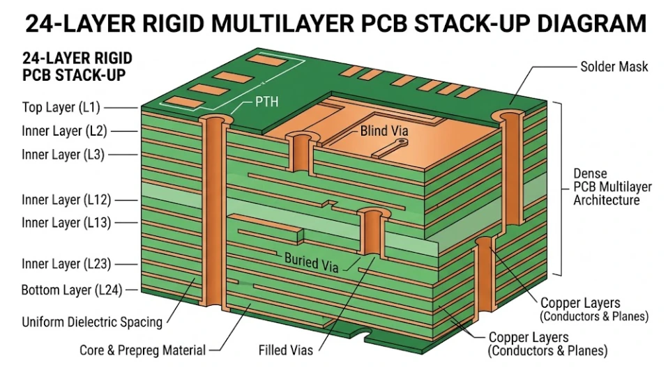
The standard PCB thickness is 1.57 mm, or 0.062 in, usually rounded to 1.6 mm. It is the default for rigid FR-4 boards because it fits most through-hole leads, card guides, and connectors, and it is the thickness most stackups and fabrication lines are set up around. If you leave thickness off an order, a board house will usually assume it.
1.6 mm is a default, not a rule. Common alternatives are 0.8, 1.0, 1.2, 2.0, and 2.4 mm, and thinner or thicker boards are built when the product needs them. What matters is that the finished thickness, its tolerance, and the stackup that produces it agree with each other and with the parts that mount to the board.
This guide covers the standard printed circuit board thickness and why it exists, which thicknesses are common at each layer count, how tolerance works, how special PCB types change the picture, when to go thinner or thicker, and how to specify board thickness in an RFQ.
Key takeaways
- Standard PCB board thickness is 1.57 mm (0.062 in), commonly called 1.6 mm.
- APT's standard multilayer stackup catalog covers 0.4 to 2.4 mm for 4 to 18 layers; advanced builds reach 0.2–6.0 mm.
- Not every thickness is available at every layer count. More layers need more material, so very thin boards with many layers are not standard.
- Thickness tolerance in APT's catalog is ±10% of finished thickness. Tighter tolerance is possible but must be stated and reviewed.
- Card-edge connectors, press-fit pins, and slots often fix the thickness and tolerance before anything else does. Start from those.
- Flexible, ceramic, heavy-copper, and high-frequency PCBs have their own thickness ranges that differ from standard rigid FR-4.
What is the standard PCB thickness?
The standard PCB thickness is 1.57 mm (0.062 in). The number comes from early laminate stock sold in 1/16-inch sheets. Exactly 1/16 in is 1.5875 mm; the industry rounds to 0.062 in, which is 1.57 mm, and metric systems often list it as 1.6 mm. In practice, a "1.6 mm" board and a "62 mil" board are the same order.
It became the standard because it balances stiffness and weight, suits the lead lengths of most through-hole parts, and matches the card-edge and board-to-board connectors designed around it. APT's own stackup catalog shows the same pattern: the regular 4, 6, 8, and 10-layer builds all start at 1.6 mm.
What does finished thickness include?
Finished thickness is the total thickness of the completed board, normally measured across the laminate, copper, and plating. Whether solder mask and surface finish are included in the measurement is something to confirm with the fabricator, because on a board with a tight tolerance it can make a difference. If you specify a thickness at a particular location, such as across card-edge fingers, say so on the drawing.
Common PCB thicknesses by layer count
These are the finished thicknesses offered in APT's standard multilayer PCB stackup catalog, by layer count. "Available" means at least one catalog stackup exists at that thickness; other values can be built on a custom stackup after review.
| Layer count | Catalog thicknesses (mm) | Notes |
|---|---|---|
| 4 layers | 0.4, 0.6, 0.8, 1.0, 1.2, 1.6, 2.0, 2.4 | Widest range; thin builds use thin cores and prepregs |
| 6 layers | 0.6, 0.8, 1.0, 1.2, 1.6, 2.0, 2.4 | 1.6 mm and above have the most stackup options |
| 8 layers | 1.0, 1.2, 1.6, 2.0, 2.4 | Thin options narrow as layers are added |
| 10 layers | 1.0, 1.2, 1.6, 2.0, 2.4 | Most catalog builds at 2.0 and 2.4 mm |
| 12 layers | 1.2, 1.6, 2.0, 2.4 | |
| 14 to 18 layers | 2.0, 2.4 | Higher layer counts need more total dielectric |
APT's advanced multilayer builds cover 0.2–6.0 mm total board thickness (documented in production records for 8–236 mil cores). For backplane and extra-thick builds, the multilayer PCB page lists thicknesses from 0.2 to 6.0 mm, and the backplane page covers 3.4 to 7.0 mm.
Single and double-sided boards are usually made from a single core, so their thickness follows the core thickness chosen plus copper. Thin flexible circuits and rigid-flex boards have separate ranges covered below.
Why thin boards stop at a layer count
Each copper layer and each dielectric layer takes up thickness, and dielectrics cannot be made arbitrarily thin without affecting impedance, voltage withstand, and lamination quality. As layer count rises, the minimum practical thickness rises with it. That is why the catalog has 0.4 mm only for 4-layer boards and starts 14 to 18-layer builds at 2.0 mm.
PCB thickness tolerance
Thickness tolerance is the allowed difference between the nominal and the measured finished thickness. APT's stackup catalog states ±10% of finished thickness for each entry. For a 1.6 mm board, that is a range of 1.44 to 1.76 mm.
Tolerance comes from several sources added together: variation in core and prepreg thickness, resin flow during lamination, copper plating thickness, and finish. A board built from more layers stacks up more of that variation.
When ±10% is not enough — for example for a card-edge connector with a narrow thickness window — state the required tolerance on the drawing and where it is measured. The fabricator then chooses materials and a stackup to hit it, or tells you before production that it cannot be held.
Choosing PCB thickness: thin vs thick boards
This table sets out when each band of thickness makes sense and what it changes. The thickness bands use APT's catalog values; costs are relative, because pricing depends on the full stackup and quantity.
| Finished thickness | Typical reasons to choose it | What changes | Cost relative to a standard 1.6 mm build |
|---|---|---|---|
| 0.4–0.8 mm | Thin products, modules, wearables, space-limited enclosures | Board flexes more; warpage and handling during assembly need attention; fewer layer options | Similar at low layer count; can rise when thin materials or carriers are needed |
| 1.0–1.2 mm | Compact products that still need rigidity | Moderate stiffness; some connectors are designed for this range | Similar |
| 1.57–1.6 mm (standard) | Default for most rigid boards, through-hole parts, card guides | Most stackups and connector footprints assume it | Baseline |
| 2.0–2.4 mm | Higher layer counts, heavy parts, extra stiffness, some press-fit connectors | Higher aspect ratio for the same drill size | Usually higher, driven by layer count and material |
| Above 2.4 mm | Backplanes, high layer count, mechanical loads | Aspect ratio and drilling become limiting; long lamination cycles | Higher; custom stackup required |
Thickness and aspect ratio
Thicker boards make plated holes deeper. APT's drilling records list 10:1 to 12:1 as the standard production aspect ratio for mechanical drilling. At 1.6 mm, a 0.15 mm drill already sits near the top of that range. If you increase thickness, check the smallest via drill again. The PCB via guide explains how aspect ratio limits via size.
Thin boards in assembly
Thin boards bend under their own weight in a reflow oven and can warp after soldering. They may need support or carriers during assembly, and panel design matters more. The assembly line should know the thickness in advance. See the reflow soldering process guide and solder joint defects for how to manage warpage during production.
Thickness for flexible, ceramic, and specialty PCBs
Standard multilayer thickness ranges do not apply to specialty board types. Each has its own practical range driven by different material systems and applications.
Flexible PCB thickness
Flexible circuits are measured differently. The total board thickness for flex is the sum of the polyimide or LCP base, copper layers, and coverlay. APT's flex data records show total flex thicknesses down to 0.05 mm (50 µm) for ultra-thin single-sided builds. Most flex circuits land in the 0.05–0.20 mm range depending on layer count and copper weight. Thicker polyimide builds can reach 0.3 mm or more.
Rolled annealed copper is the main driver of flex thickness variation: 12.5 µm RA copper gives a thinner board than 105 µm (3 oz) ED copper. Adding coverlay (12–50 µm polyimide) and stiffeners (FR-4 or stainless steel at various thicknesses) brings component areas back up toward rigid thickness. For more on flex materials, see the what is copper-clad laminate guide.
Ceramic PCB thickness
Ceramic substrates are measured by their raw slab thickness before patterning. APT's ceramic PCB records show standard substrate sizes up to 190 × 140 mm, with thickness typically ranging from 0.25 mm to 1.5 mm per substrate layer. Multilayer ceramic builds (using low-temperature co-fired ceramic, LTCC) stack multiple layers, reaching total thicknesses of 1–5 mm depending on layer count.
DPC (direct plated copper) and DBC (direct bonded copper) ceramic builds typically use 0.25–0.635 mm (10–25 mil) alumina substrates as the base. The copper circuitry adds a further 35–300 µm on each side depending on the process. For a ceramic PCB product page with full thickness data, see the ceramic PCB capability page.
Heavy copper and power PCB thickness
Boards built for high current have different thickness trade-offs. APT's heavy copper PCB records document finished board thicknesses from 0.8 mm to 6.0 mm for 2–10-layer heavy copper builds. Thicker boards help with thermal spreading from power devices, but they also increase drilling cost and aspect ratio constraints.
The relationship between board thickness and copper weight is not simple: heavier copper requires wider trace spacing, which in turn may require a thicker board to maintain dielectric spacing. APT's engineering team reviews copper weight and thickness together before releasing a heavy copper order.
High-frequency PCB thickness
High-frequency and RF PCBs on Rogers/PTFE or hydrocarbon materials have a total board thickness range documented from 0.2 mm to 10.0 mm in APT's RF capability records. Thin RF boards (0.2–0.5 mm) are common for antennas and planar circuits where the substrate itself acts as the microwave medium. Thicker builds serve power combines and multi-layer RF modules.
The dielectric constant of the RF material is more important than the thickness alone: a 0.254 mm RO3003 board and a 0.508 mm RO3003 board both work as antennas, but at different frequencies and with different bandwidth. Thickness affects impedance (through its effect on trace width for a given dielectric and impedance target), so confirm the stackup with the fabricator before laying out critical RF traces.
Rigid-flex PCB thickness
Rigid-flex boards combine thin flex sections with rigid sections, so there is no single thickness number — each zone has its own. APT's rigid-flex records show flex zones at 0.05–0.20 mm total thickness (thin polyimide cores with RA copper and coverlay) and rigid zones at 0.8–2.4 mm following the standard multilayer ranges above. The transition between them requires careful planning: a gradual thickness taper is preferred to avoid stress concentrations at the flex-to-rigid boundary.
Connectors, gold fingers and slots
Connectors often decide thickness before anything else in the design.
- Card-edge connectors. A board that plugs into a card-edge socket must match the socket's specified board thickness and tolerance at the fingers. Check the connector datasheet, not the board default.
- Press-fit connectors. Press-fit pins are designed for a range of board thicknesses and a finished hole tolerance. APT's drilling records list ±0.05 mm finished-hole tolerance for press-fit holes.
- Board-to-board and mezzanine connectors. These set stack heights that include board thickness.
- Slots, tabs, and enclosure features. Mechanical parts that fit into slots or rails depend on board thickness and edge profile.
- Bevels and edge profiles. A bevelled card edge depends on the finished thickness at the edge. APT's PCB profiling page asks for the insertion edge, finished thickness, bevel angle and depth, and hard-gold region for card-edge bevels.
When one of these applies, write the thickness and tolerance at that feature into the fabrication drawing.
How stackup sets finished thickness
The finished thickness is the sum of everything in the stackup: cores, prepregs, copper on each layer, plating, and the outer finish. You can design that sum two ways:
- Choose a standard catalog stackup at your target thickness, which fixes core and prepreg choices and makes impedance easier to predict.
- Design a custom stackup, choosing core and prepreg thicknesses to meet impedance and other needs, then adjust to reach the target thickness.
Copper weight affects the result. APT's catalog lists 1 oz copper at approximately 0.035 mm per layer before plating, and heavier copper adds proportionally more. Inner layer copper ratio also matters: prepreg flows into the gaps between traces during lamination, so a sparse copper layer consumes more resin and the finished stack ends up thinner.
For how the layers are arranged, see the PCB stackup design guide. For core and laminate choices, see what copper-clad laminate is.
Specifying thickness in the RFQ
A complete thickness callout prevents most surprises:
- Finished board thickness, nominal value, and tolerance (for example 1.6 mm ±10%, or a tighter value where needed)
- Where thickness is measured, and whether it includes solder mask and finish, if it matters to your fit
- Thickness at specific features, such as card-edge fingers, if that differs from the general tolerance
- Layer count and copper weight on each layer
- Stackup drawing, or a statement that the fabricator's standard stackup is acceptable
- Material requirement (for example FR-4 with a Tg grade), because laminate availability affects which thicknesses are possible
- Controlled impedance targets, since thickness changes dielectric spacing and therefore impedance
- For flexible or rigid-flex sections: thickness per zone rather than a single board value
Why work with APTPCB on board thickness?
APT reviews thickness, layer count, copper weight, and stackup together before release, so the finished board meets the drawing and the impedance target at the same time. The standard 4 to 18-layer stackup catalog covers 0.4 to 2.4 mm builds, and custom stackups are reviewed when your design needs a different thickness or tighter tolerance. For specialty boards, APT's flex, ceramic, heavy-copper, and RF engineering teams each have their own thickness and material records. For FR-4 builds, the FR4 PCB manufacturing team can confirm the closest standard stackup to your target before you finalize layout.
Relevant industry standards for rigid PCB thickness include IPC-2221 (generic standard on printed board design), IPC-6012 (qualification and performance of rigid printed boards), IPC-A-600 (acceptability of printed boards), and IPC-6013 (flexible rigid printed board qualification and performance). These define acceptability criteria and inspection methods but do not mandate a specific thickness.
Start from what the board plugs into
For most designs, 1.6 mm is the right answer and needs no further thought. When something mechanical depends on the board — such as a card-edge socket, a press-fit connector, or a thin enclosure — let that part set the thickness and tolerance first. Then choose a stackup that reaches it, and write all of it on the fabrication drawing.
Frequently asked questions
What is the most common PCB thickness?
The most common PCB thickness is 1.57 mm (0.062 in), usually called 1.6 mm. It is the default for rigid FR-4 boards, and most connectors, card guides, and stackups are designed around it.
Is 1.6 mm the same as 0.062 inches?
Effectively, yes. 0.062 in converts to 1.57 mm, and metric ordering systems usually round it to 1.6 mm. Both describe the same standard board thickness. With a typical ±10% tolerance, the difference is well within the allowed range.
What thickness is a 4-layer PCB?
A 4-layer PCB is most often 1.6 mm thick, but it can be built thinner or thicker. APT's standard catalog lists 4-layer builds from 0.4 mm to 2.4 mm, including 0.8, 1.0, 1.2, and 2.0 mm.
What is the typical PCB thickness tolerance?
APT's standard stackup catalog states ±10% of finished thickness, which gives 1.44 to 1.76 mm for a 1.6 mm board. Tighter tolerances can be requested where a connector or enclosure needs them, and should be stated on the drawing with the measurement location.
Does a thicker PCB cost more?
Usually a little, but layer count and material drive cost more than thickness alone. A thicker board may also need larger drills to stay within aspect-ratio limits. Very thin boards can add cost when they need special materials or carriers during assembly.
Can I choose a non-standard PCB thickness?
Yes. Non-standard thicknesses are built on a custom stackup after an engineering review. State the nominal value, tolerance, layer count, and copper weights so the fabricator can confirm materials and impedance before production. For specialty boards such as flex, ceramic, or heavy copper, the practical thickness ranges differ from standard FR-4.