
A PCB trace is a shaped copper path that carries an electrical connection across a printed circuit board. It can connect component pads on one copper layer, or reach a via that continues the connection onto another layer.
For an engineer or buyer, the useful question is not just “Can I see a line?” It is whether the intended copper path is continuous, belongs to the right net, stays clear of other conductors, and is suitable for its electrical and thermal job. A photograph or a passed continuity test answers only part of that question.

Photo: Tima Miroshnichenko / Pexels. The image shows a real board surface, but provides no scale and cannot establish trace width, electrical nets, current capacity, or an APTPCB source.
Trace, pad, via, and copper pour: different jobs
A trace is usually recognizable in a layout as a relatively narrow copper route between electrical features. Its shape may include straight segments, corners, branches, or changes in width.
The neighboring features have different purposes:
- Pad: A copper feature associated with a connection point. A surface-mount component pad, for example, provides an area for a soldered terminal. Pads can also occur at plated holes and other features.
- Via: A plated hole used to connect selected copper layers. A via can transfer a signal from an outer layer to an inner layer, even though the path beyond it is hidden from view.
- Copper pour: A larger copper region generated from a defined area in the design, often assigned to a power or ground net. It may connect to traces, pads, and vias, but it is not simply a wide trace. Clearance rules and connection settings determine where the pour actually forms copper.
- Solder mask: A protective coating over much of the outer copper. It is not the copper conductor and should not be mistaken for trace thickness. Openings in the mask expose selected areas, such as component pads.
A copper pour can be interrupted by clearances, slots, other nets, or board edges. A region that looks connected in an unfilled layout may become isolated after the CAD tool fills it. Conversely, a trace can connect to a pour if both are on the same net and the design settings create the intended junction.
For the broader board structure behind these features, see what a PCB is.
Follow one hypothetical net across layers
Invented example: Assume a sensor has a signal output pad on the top side of a multilayer board. The designer wants to connect it to a receiving component’s input pad, also on the top side.
The intended route is:
- The sensor pad connects to a top-layer trace.
- That trace reaches a via assigned to the same signal net.
- The via connects to an inner-layer trace.
- The inner trace reaches a second via.
- The second via connects to a top-layer trace ending at the receiver pad.
All of these copper features are intended to belong to one signal net. The second via is needed in this example because the route returns to a top-side pad; a different design could end elsewhere.
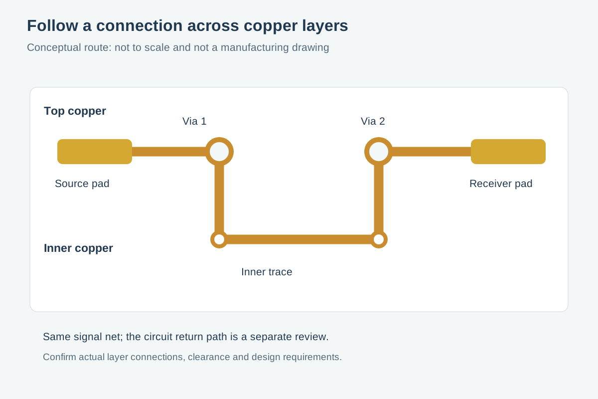
Conceptual illustration of PCB routing features and layer transitions, not a manufactured board or a scale drawing.
To check the example in CAD, follow the net from pad to pad rather than checking only the visible top trace. Confirm that both vias connect to the intended layers, the inner segment is present, and no unwanted gap remains. Also check that the net is not shorted to a different net.
A net name expresses design intent; it does not by itself prove the exported copper geometry or a finished board has the intended connection. Design-rule checks, file review, and any agreed electrical test each provide different evidence.
The signal route is not the whole return path
The sensor signal also has a return-current path through the rest of the circuit. In this example, the signal trace and its vias are one net; the return path is separate and may use ground copper and other circuit connections.
At faster signal transitions, the return current’s distribution is influenced by nearby reference conductors. If the signal changes layers, the designer should examine the reference arrangement at that transition too. A continuous signal trace does not guarantee that its return path has a good nearby route.
That distinction matters when the route passes a plane split, a gap in a ground pour, or a change from one reference layer to another. Depending on the circuit and stackup, the designer may need to change the routing or provide an appropriate connection between reference regions. The correct solution depends on the actual layout, not on the presence of a via alone.
What the reader should check
The following checks answer different questions. Passing one does not make the others unnecessary.
| Check | What to look for | If the condition is not met |
|---|---|---|
| Net connectivity | Pads, traces, pours, and vias belong to the intended net and form an unbroken route on the intended layers. | Trace the route in CAD, inspect unconnected items, and correct the geometry or net assignment before releasing files. |
| Clearance | Copper belonging to different nets remains separated under the applicable design rules. Check around pads, vias, pours, and board features. | Resolve the rule violation or obtain an engineering decision based on the voltage, environment, and applicable requirements. |
| Current and heating | The complete current path, including narrow segments, transitions, and copper thickness, is suitable for its operating conditions. | Review the limiting sections and assumptions; do not judge the path by its widest segment alone. |
| Signal reference | For a signal sensitive to return-path geometry, examine nearby reference copper and layer transitions. | Review splits, voids, and reference changes with the circuit and stackup; reroute or revise the reference arrangement as needed. |
| Copper and mask | The copper layer defines the conductor; mask openings and coverage are checked separately. | Correct mismatched or unintended openings without treating a mask edit as a copper-width change. |
| Manufacturing outputs | Layer files, drills, stackup, and drawing describe the same board revision. | Stop the release and resolve conflicting files or notes rather than asking the fabricator to guess. |
These checks apply to a simple sensor route as well as a more demanding design. The depth of review depends on the circuit, operating conditions, and consequences of failure.
Width is not clearance
Trace width is the width of the copper path itself. Clearance is the separation between features that must not connect, such as copper on different nets. Increasing one does not automatically establish a suitable value for the other.
Width can affect resistance, heating, and signal behavior. Clearance helps prevent unintended electrical interaction or breakdown, but its required value depends on factors such as voltage, environment, surface condition, and the rules or standards chosen for the product.
If a clearance warning appears, first identify which nets and physical features are involved. Then check whether it is a genuine design issue, a rule-setup error, or an intentional feature requiring documented review. Suppressing the warning without resolving its cause leaves the manufacturing handoff ambiguous.
Copper thickness is not solder-mask thickness
The copper thickness used for a trace is part of the conductor’s geometry. Solder mask is a separate coating, typically covering much of the outside of the board while leaving openings where needed.
A trace that appears broad beneath colored mask cannot be measured reliably from a normal photograph. Nor can its copper thickness be inferred from the mask color. Use the design data and agreed fabrication requirements, including any relevant finished-copper requirements, rather than appearance.
Three decisions that are often confused
1. Can the path carry the required current?
The thermal question is whether the whole path can carry the required current under the intended conditions without an unacceptable temperature rise or other problem.
Width and copper thickness matter, but so do the route length, nearby copper, layer position, board construction, ambient conditions, duty cycle, and connections. Vias and local neck-downs deserve attention as well. A wide pour connected through a narrow segment is still limited by more than the pour alone.
There is no universal safe current-per-width rule in this article. When current or heating is important, document the operating conditions and use an appropriate engineering method. The heavy copper PCB design and IPC-2152 discussion provides a starting point for that separate review.
2. Does a signal have a suitable reference and impedance?
Not every signal trace needs to be treated as a controlled-impedance transmission line. The decision depends on signal transition times, route length, the circuit’s tolerance for reflections, and the intended stackup.
When impedance or return-path behavior is important, width alone is not enough. Copper geometry, spacing to reference copper, dielectric properties, and the surrounding structure all matter. A trace may be continuous yet still have an unsuitable reference path or impedance.
Review the PCB stackup design alongside the route. If controlled impedance is required, put the requirement and applicable tolerances in the design package rather than assuming the fabricator can infer them from a line on a drawing.
3. Is there enough separation for the voltage?
Voltage clearance is a different decision from thermal current or signal impedance. The concern is whether the separation and insulation are appropriate for the operating and transient voltages and the expected environment.
A trace can be wide enough for current and still be too close to another conductor. Conversely, generous spacing does not prove that the trace can carry its current. If the product has applicable safety or insulation requirements, identify them explicitly and review the relevant spacing in the actual design.
Why vias and inner layers need special attention
On a multilayer PCB, an outer trace may disappear at a via and continue inside the board. A surface inspection cannot show the complete inner-layer route.
The via’s plated barrel and associated copper features provide the intended interlayer connection. On a copper layer where the via must not connect, an opening in surrounding copper—often called an antipad—provides separation. The required geometry depends on the design and layer construction.
For a layer change, check both sides of the decision:
- Intended connection: Does the via connect to the correct trace or copper region on each intended layer?
- Intended isolation: Is it separated from unrelated copper on layers where no connection is wanted?
- Reference continuity: If the signal is sensitive to return-path discontinuities, what happens to its reference at the transition?
- Physical requirements: Are the via and drill details consistent across the layout, fabrication files, and drawing?
AMD’s UltraScale Architecture PCB Design User Guide, in its “Pads and Antipads” discussion, describes these copper and clearance concepts. The exact via structure and rules should come from the actual design, not from a generic cross-section.
What electrical continuity testing can—and cannot—show
A PCB electrical continuity test checks for an electrical connection between specified points under the test method and conditions. An agreed bare-board electrical test may also check for unintended shorts. The netlist, test coverage, access, and acceptance criteria matter: a result is only as useful as the points and conditions included.
A continuity pass does not, by itself, prove that:
- The trace can carry its operating current without excessive heating.
- Controlled impedance is within a required tolerance.
- The return-current path is suitable for the signal.
- A component has been correctly soldered or the assembled product works.
- The board will meet every environmental or lifetime requirement.
If the design review and test result disagree—for example, an expected route is open—hold the affected material and compare the tested netlist, board revision, test access, and released fabrication data. Determine whether the issue is in the design, file preparation, test setup, or board before deciding on disposition. Do not treat a retest alone as an explanation of the failure.
What to send with a trace-sensitive RFQ
A useful request for quotation gives APTPCB enough information to understand the board and identify questions before fabrication. Include the following where applicable:
- Fabrication drawing: Board identification and revision, outline, applicable notes, and required acceptance criteria.
- Copper-layer information: Layer count, ordered stackup, layer identification, and specified copper requirements. Identify any controlled-impedance structures and their requirements.
- Complete design outputs: A consistent set of Gerber files with NC drill data, or a complete ODB++ or IPC-2581 package. Include layer mapping and drill information so the files can be interpreted together.
- Other fabrication layers: Solder mask, legend, board profile, and other necessary outputs, clearly distinguished from copper.
- Specified requirements: Relevant material, finish, tolerances, electrical-test requirements, and applicable standards or revisions.
- Special concerns: Identify current-carrying nets, sensitive signals, unusual via structures, or clearance-critical areas that require engineering discussion. State the assumptions or operating conditions behind those concerns.
If the drawing conflicts with a file, or the stackup does not match the layer outputs, resolve the discrepancy before authorizing production. For wider layout preparation, see the PCB design guide.
Use the quote page to start an RFQ, or contact APTPCB to discuss a question about the handoff.
Public references
- Cornell University, PCB Layout.
- AMD, UltraScale Architecture PCB Design User Guide (UG583), “Pads and Antipads.”
- Analog Devices, AN-136: PCB Layout Considerations for Non-Isolated Switching Power Supplies.