
A six-layer PCB can give you more room to route signals and distribute power than a simpler construction, but the layer count alone does not tell you how well the board will perform. The useful decision is how to assign the copper layers, where critical signals will return, and whether the fabricator can build and verify the proposed geometry.
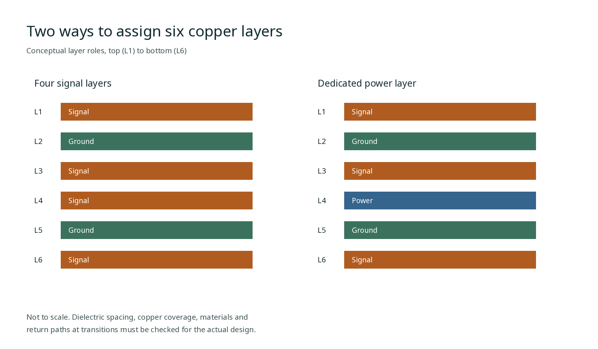
Consider two conceptual layer-role arrangements, from top L1 to bottom L6:
- S-G-S-S-G-S: four signal-designated layers and two ground-designated layers.
- S-G-S-P-G-S: three signal-designated layers, two ground-designated layers, and one power-designated layer.
Neither is a fabricated cross-section. The roles do not specify copper thickness, dielectric spacing, material, or how much copper remains after routing and clearances. Power traces or pours can exist in either arrangement; a signal-designated layer is not necessarily signal-only.
Layer roles only, not a physical cross-section or a build specification.
For broader architectural choices, see PCB stackup design.
A hypothetical design to compare
Suppose you are designing a rigid board with:
- Critical routes on both external layers.
- At least one critical route that must use an internal layer.
- Multiple power rails that need to reach components across the board.
You have not yet selected dimensions or materials. Your immediate task is to choose a starting layer arrangement and identify what must be checked before handoff.
Option 1: S-G-S-S-G-S
| Layer | Conceptual role |
|---|---|
| L1 | Signal |
| L2 | Ground |
| L3 | Signal |
| L4 | Signal |
| L5 | Ground |
| L6 | Signal |
This arrangement gives the hypothetical design two internal signal-designated layers. L3 sits next to L2 ground, while L4 sits next to L5 ground. That extra internal routing option may help when external critical routes and other connections compete for space.
The middle signal layers are also adjacent to each other. Whether routes on L3 and L4 couple significantly depends on the actual geometry and routing, so check their relationship rather than assuming the ground layers isolate them.
There is no dedicated power-designated layer in this arrangement. The multiple rails still need to be distributed using suitable copper, such as traces or pours, subject to the available routing space and electrical requirements. Those copper shapes can also affect the reference coverage available to nearby signals.
Option 2: S-G-S-P-G-S
| Layer | Conceptual role |
|---|---|
| L1 | Signal |
| L2 | Ground |
| L3 | Signal |
| L4 | Power |
| L5 | Ground |
| L6 | Signal |
This arrangement gives the hypothetical design a power-designated layer, but only one internal signal-designated layer. It may be a useful starting point when distributing the multiple rails is a major concern and L3 has enough routing capacity for the internal signals.
L3 is between L2 ground and L4 power, so a route on L3 can couple to both. Do not describe it as having an exclusively ground reference without checking the actual copper and spacing. If part of the return current uses the power copper as a reference, the design also needs a suitable AC return path to ground. The power distribution and decoupling arrangement must be considered as part of that path.
A power-designated layer also does not imply one uninterrupted plane. Multiple rails may require separate copper regions and clearances. Check how those boundaries affect L3 routes and their return paths.
How to choose for the example
Start by assigning the known critical routes, not by declaring one arrangement better:
- Place the external routes. In both options, L1 is adjacent to L2 ground and L6 is adjacent to L5 ground. Check that ground copper is actually present beneath each critical route, including around clearances and other interruptions.
- Place the internal route. In the first option, consider L3 against L2 ground or L4 against L5 ground, while also checking the adjacent internal signal layer. In the second, place the route on L3 and assess both the L2 ground and L4 power copper around it.
- Map the power rails. Compare the routing and copper area they require in both options. In the second option, examine proposed rail boundaries on L4; in the first, examine how power traces or pours compete with signal routing and reference copper.
- Inspect layer transitions. A route changing layers also changes the environment for its return current. Check the complete path around each transition, not just the signal via.
For example, if a critical route moves from L1 to L6, its adjacent ground-designated layer changes from L2 to L5. A proposed ground connection near the transition may help provide a return path, but its suitability depends on the actual copper, via placement, and geometry. Similarly, a transition involving a power reference requires a suitable AC path between that power copper and ground.
For a ground-to-ground transition, sketch the signal and ground connections together:
                 signal via    ground via
L1  signal  ---------+             |
                     |             |
L2  ground  ---------|-------------+
                     |             |
L3  inner copper     |             |
                     |             |
L4  inner copper     |             |
                     |             |
L5  ground  ---------|-------------+
                     |             |
L6  signal           +---------    |
The vertical ground connection represents a nearby plated via joining L2 and L5 copper on the same ground net. The drawing does not show clearances, other via layers or the full current path. Check the actual plane connectivity, via placement, antipads and critical-net geometry. The via's presence alone does not establish an adequate return path.
The better option is the one that accommodates the example’s routes and rails after these checks, with geometry the fabricator confirms. The conceptual layer order alone cannot establish that.
For more on planning ground and power copper, see ground and power PCB design. The high-speed PCB design guide discusses routing and return-path considerations for critical signals.
Per-critical-net checklist
Use this checklist for each critical net, including each portion on a different layer:
- Signal layer: Which layer carries the route, and where does it change layers?
- Adjacent reference: Which adjacent ground or power copper can the route couple to? For L3 in S-G-S-P-G-S, consider both adjacent layers.
- Actual coverage: Is the relevant copper present along the route, rather than merely assigned a ground or power role?
- Voids and boundaries: Do clearances, copper voids, or rail boundaries interrupt or change the available reference?
- Transition return path: How can return current travel when the signal changes layers or reference copper? If power is involved, what provides the AC path to ground?
- Fabricator-confirmed geometry: Have the actual copper, spacing, materials, and fabrication tolerances for the proposed build been confirmed?
- Verification: What analysis, checks, or measurements are agreed for the net and construction, and who will review the results?
A layer diagram by itself does not answer these questions.
Confirm the build before committing to dimensions
Send the preferred arrangement to the fabricator as a starting proposal. Ask for a buildable stackup with project-specific materials, board thickness, copper, spacing, and tolerances, then compare the returned construction with the critical-net assumptions.
Check that the thicknesses add up
This arithmetic example uses six nominal 0.035 mm copper layers. It illustrates a thickness check for the first layer-role arrangement; it is not an APTPCB standard build, a finished-board thickness guarantee or an impedance design.
| From top to bottom | Nominal thickness (mm) |
|---|---|
| L1 signal copper | 0.035 |
| L1–L2 dielectric | 0.100 |
| L2 ground copper | 0.035 |
| L2–L3 dielectric | 0.200 |
| L3 signal copper | 0.035 |
| L3–L4 dielectric | 0.500 |
| L4 signal copper | 0.035 |
| L4–L5 dielectric | 0.200 |
| L5 ground copper | 0.035 |
| L5–L6 dielectric | 0.100 |
| L6 signal copper | 0.035 |
| Nominal total | 1.310 |
The calculation is 6 × 0.035 mm of copper plus 1.100 mm of dielectric. It excludes solder mask, surface finish and variation from plating and manufacturing. Actual copper distribution, dielectric construction, press-out and tolerances require fabricator review. This table alone gives neither a line width nor an impedance value.
Also discuss symmetry in the actual construction. It is a manufacturing consideration worth reviewing, but a nominally symmetric layer plan is not a guarantee against warpage.
If impedance is part of the project, agree on the target, tolerance, and verification approach with the fabricator. A test coupon can support an agreed impedance check for the construction; it does not verify every route on the finished board. See how to read an impedance coupon TDR report for help interpreting that evidence.
Document the final layer roles and the assumptions that affect critical routes alongside the confirmed build. The stackup documentation guide covers the handoff in more detail.
To discuss a proposed construction, request a quote or contact APTPCB with the layer arrangement, critical-net requirements, and questions that still need fabricator confirmation.
Technical references
Texas Instruments documents SCAA082A and SPRU889 are relevant primary references for high-speed PCB layout and interface considerations. Apply their guidance to the actual circuit and confirmed construction rather than treating either conceptual arrangement above as a finished specification.