
mSAP is worth discussing with a fabricator when your routing cannot be achieved with the finished trace width, spacing, copper thickness and registration available from a practical subtractive process. It is not a substitute for a complete stackup review: the supplier must confirm the geometry and tolerances for your specific dielectric, copper construction, via design and application.
For an IC package substrate, the question extends beyond fine lines. The construction must support the package interfaces and the evidence needed for package qualification. A substrate-like PCB may need similarly careful routing control but serve a different interface, while a conventional PCB may meet its requirements without a semi-additive process. The advanced PCB materials and substrates guide discusses those material and qualification boundaries in more detail.
Ask potential suppliers which construction they propose, what finished geometry they can control, and what evidence they can provide for the actual stackup.
What mSAP does
Modified semi-additive processing, or mSAP, is a family of copper patterning processes commonly built around a thin copper base. In a simplified flow, the fabricator:
- Starts with a construction that has a thin copper base.
- Applies and patterns resist to define where copper will remain.
- Plates copper into the exposed pattern.
- Removes the resist.
- Uses a final flash etch to remove unwanted exposed copper between features.
The details depend on the construction and the factory. In particular, the copper removed during the final etch is not necessarily limited to the original base copper; deposited copper may also contribute to the material removed.
Flash plating and flash etching are different operations. Flash plating adds a thin copper deposit; flash etching removes copper. An RFQ that uses “flash” without specifying the operation can leave an important process detail ambiguous.
The thin starting copper layer reduces the amount of copper that must be removed after plating, although the final etch still affects the finished features.
Subtractive, mSAP and SAP are process families
In a broadly subtractive process, the starting copper is patterned by removing unwanted copper. With finer features, the resulting trace profile and spacing depend on the starting construction and the etching process.
mSAP combines a thin copper base with patterned copper plating and subsequent removal of exposed copper. Semi-additive processing, or SAP, also uses patterned plating and may involve removal of a seed layer. The boundary between the labels is not a universal recipe, and seed removal is not exclusive to one family.
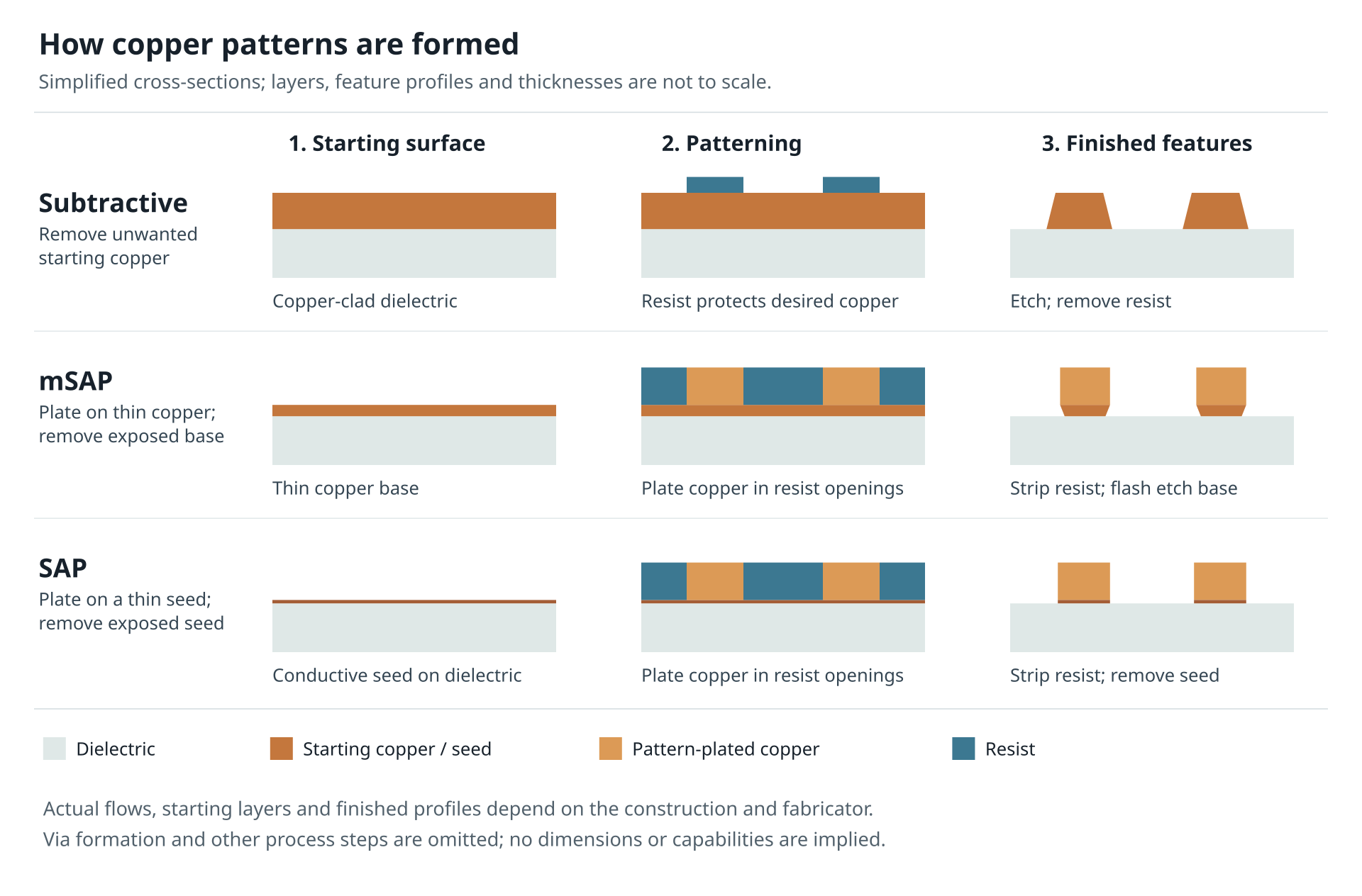
Conceptual process comparison, not to scale. Via formation and other steps are omitted; actual flows and finished profiles vary.
A process name alone therefore does not tell a designer:
- The finished trace width at the relevant points in its profile.
- The finished copper thickness and spacing.
- The registration between the pattern and its vias or adjacent layers.
- The tolerance distribution or acceptance criteria.
- Whether the construction is suitable for the application.
Ask the supplier to describe the proposed layer construction and verify the finished features instead of assuming those details from “mSAP” or “SAP.”
Why finished geometry matters
A fine-line requirement is rarely just a nominal width and space. Trace profile, copper thickness and spacing are interdependent: a process that meets a nominal width in one construction may need a different tolerance or geometry in another. The applicable dielectric and its surface also matter when assessing copper adhesion and the finished stackup.
A hypothetical cross-section
Suppose a drawing calls for a finished line width of 20 µm, with a tolerance of ±2 µm measured at the top of the conductor. A representative cross-section shows 20 µm at the top and 24 µm at the base. The top measurement meets that particular width requirement, but it says nothing by itself about whether the base width, copper thickness or space to the neighboring conductor meets the drawing. Those features need their own specified limits and measurement locations.
The example values are invented to illustrate a measurement question; they are not a design rule or a supplier capability. Agree on how and where widths and spaces will be measured, including how the section and measurement method affect the reading. Check the finished profile against the electrical design and the complete set of acceptance criteria.
Via geometry adds another constraint. The chosen via formation and fill approach must work with the layer construction, land size, registration and the routing connected to it. A trace may fit in the layout while the combination of via, land and registration allowances does not.
Electrical and thermal requirements can change the decision too. A finer line that creates routing space may not provide the copper geometry needed for the electrical design. Likewise, a copper construction selected for routing must be considered alongside the project’s thermal requirements. These trade-offs need evaluation for the actual design; no process label guarantees an electrical or thermal result.
For stackup planning, see PCB stackup design. For via-related decisions, see blind and buried via planning.
Decision aid: match the requirement to the evidence
The following constructions are examples, not prescribed process assignments. Each project may justify a different process after the supplier reviews the design.
| Example construction and binding requirement | Process choice discussion | Evidence to request |
|---|---|---|
| Package substrate: dense routing to package interfaces is binding | Ask whether the proposed subtractive, mSAP or SAP construction can support the routing, registration and via structure together. Confirm how the proposed substrate interfaces with the rest of the package. | Finished trace profile and tolerances at the specified copper thickness and dielectric; registration to vias and interfaces; via formation and fill details; representative cross-sections and application-relevant test criteria. |
| Substrate-like PCB: fine routing and a defined board stackup are binding | Compare feasible constructions rather than assuming that the finest nominal feature is the best choice. Ask how routing, copper thickness, dielectric and via structure affect the proposed process. | Controlled finished geometry for the quoted stackup; layer-to-layer and via registration criteria; cross-sections showing the relevant features; electrical and thermal evidence appropriate to the stated requirements. |
| Conventional PCB: routing is feasible, but electrical, thermal or commercial constraints govern | Determine whether a subtractive construction meets the design before specifying mSAP. If it does not, ask what changes in geometry or stackup make another process worth considering. | Stackup and finished copper tolerances, via criteria, test methods and acceptance limits relevant to the design; a feasibility response for the requested quantities and documentation. |
A package substrate, substrate-like PCB and conventional PCB have different interfaces and qualification needs, even where their line geometry appears similar. For board-level designs, the HDI PCB cost guide explains how via structures, lamination and stackup decisions affect the scope of a quotation.
Show the supplier the dense regions and identify the layers and interfaces where the smallest features are needed. A cross-section can help verify the physical construction, but electrical and thermal requirements need their own evaluation under the relevant conditions. Where a board design uses controlled impedance, the guide to reading an impedance coupon TDR report explains what the measurement can and cannot establish about actual signal paths.
Prepare the RFQ and compare responses
Give each supplier the same design information and ask it to identify proposed changes and assumptions. Include, where applicable:
- The application, construction type, package or board interfaces, project stage and quantities.
- Fabrication files and controlled drawings, with dense areas and critical tolerances identified.
- The layer sequence, dielectric requirements and finished copper thickness, including any permitted substitutions.
- Finished line width, space and profile limits, measurement locations, and critical registration between copper, vias and interfaces.
- Via locations and spans, formation and fill requirements, and applicable electrical, thermal and operating conditions.
- Required inspection methods, sampling and acceptance criteria, plus the reports, material information and representative cross-sections needed and when they are due.
Mark preliminary requirements and ask which missing inputs prevent a feasibility assessment. In the response, look for the proposed construction and the layers using fine-line processes. Check whether the cross-sections represent that construction, and how evidence for your own order will be produced. Review any stackup change against the routing and electrical requirements before accepting it.
For PCB production, the fabrication process capability guide explains when statistical evidence is useful and what to check before interpreting it. A nominal minimum line width alone does not establish that a supplier can meet the complete drawing. If a required characteristic cannot be verified, resolve the evidence gap or revise the design before release.
You can request a quote or contact APTPCB to discuss the project. Include the construction and evidence requirements above so the team can assess the request; the process choice and feasibility need confirmation for the specific design.
Define the scope of qualification
Keep fabrication evidence separate from finished package or system qualification. Dimensional inspection and construction records can support an assessment of the fabricated substrate or PCB, but they do not alone qualify the assembled package or the finished system.
The responsible teams should identify the additional verification needed for the interfaces and application conditions, and agree on ownership and acceptance criteria. This distinction is especially important when a package substrate connects to a larger carrier or system board. For that interface context, see industrial-grade CoWoS carrier substrates.